2024-07-11
한어Русский языкEnglishFrançaisIndonesianSanskrit日本語DeutschPortuguêsΕλληνικάespañolItalianoSuomalainenLatina
This content is based onJiangxie Technology STM32 VideoContent, organized.
| type | serial number | bus | Function |
|---|---|---|---|
| Advanced Timer | TIM1、TIM8 | APB2 | It has all the functions of a general timer, and additional functions such as repeat counter, dead zone generation, complementary output, brake input, etc. |
| General purpose timer | TIM2、TIM3、TIM4、TIM5 | APB1 | It has all the functions of a basic timer, and additional functions such as internal and external clock source selection, input capture, output comparison, encoder interface, master-slave trigger mode, etc. |
| Basic timer | TIM6、TIM7 | APB1 | It has the functions of timing interrupt and master mode triggering DAC |
The main function:
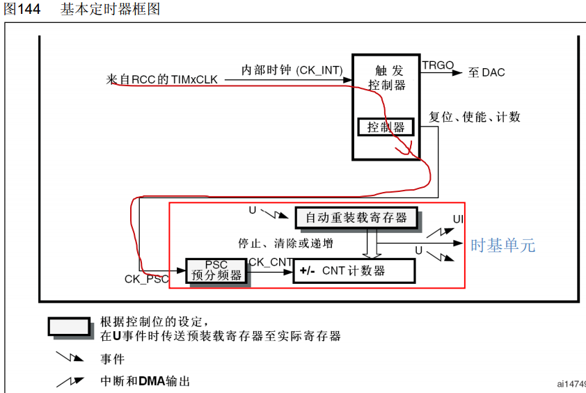
Prescaler PSC
The prescaler is connected to the input of the base count clock. Since the basic timer can only select the internal clock, it can be considered that the input line of the prescaler is connected to the internal clock (CK_INT).
The source of the internal clock is TIMxCLK of RCC, and the frequency value here is generally the system's main frequency of 72MHz.
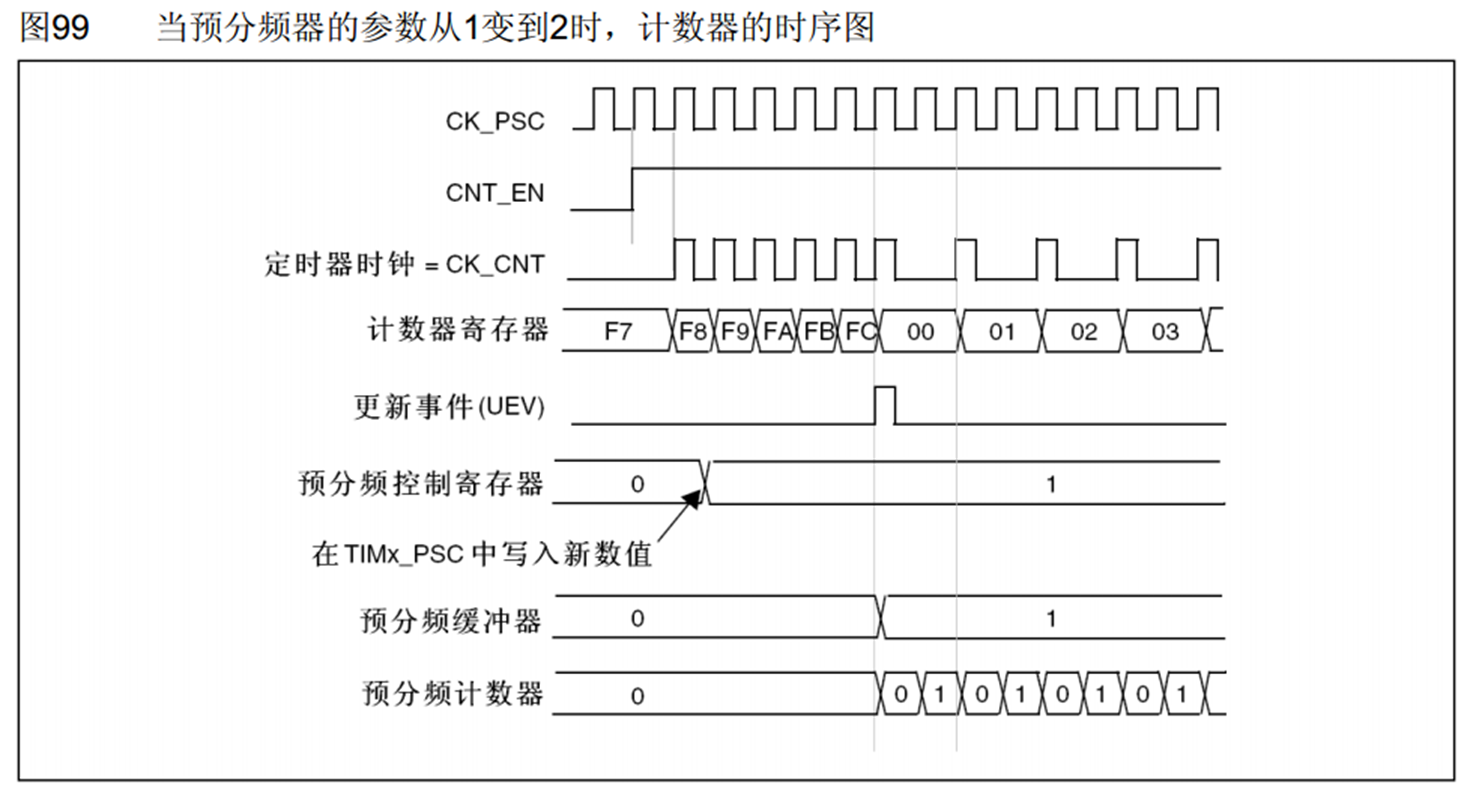
If the pre-divider is written as 0, it means no frequency division; if it is written as 1, it means 2 frequency division, and the output frequency = input frequency/2 = 36MHz.
Writing 2 means division by 3, output = input/3. Therefore, the difference between the value of the prescaler and the actual division factor is 1, and the actual division factor = the value of the prescaler 1. The prescaler is 16 bits, so the maximum value that can be written is 65535, which is 65536 division.
Counter CNT
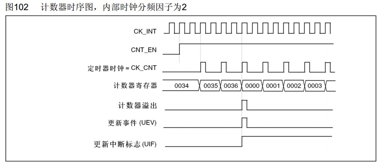
The counter can count the pre-divided counting clock. Every time the counting clock rises, the counter value increases by 1. The counter is also 16 bits, so the value inside can be increased from 0 to 65535. If it is increased again, the counter will return to 0 and start again. Therefore, the value of the counter will continue to increase during the counting process. When the increment reaches the target value, an interrupt will be generated, and the timing task will be completed. Therefore, a register is required to store the target value, which is the automatic reload register.
Auto-reload register
The auto-reload register is also 16 bits, and it stores the count target to be written. During the operation, the count value continues to increase, and the auto-reload value is a fixed target. When the count value is equal to the auto-reload value, that is, the timing time is up, it will generate an interrupt signal and clear the counter, and the counter will automatically start the next count timing.
U and UI Arrows
The upward arrow in the figure indicates that an interrupt signal will be generated here. The interrupt generated when the count value is equal to the auto-reload value is generally called an "update interrupt". This update interrupt will then lead to the NVIC. If we configure the NVIC timer channel, the timer update interrupt will be responded to by the CPU. The downward arrow indicates that an event will be generated, and the corresponding event here is called an "update event". The update event will not trigger an interrupt, but it can trigger the operation of other internal circuits.
The main function:
16-bit up, down, up/up auto-reload counter
16-bit programmable prescaler, used to divide the input clock by any factor between 1 and 65536
4 independent channels:
Synchronous circuits that use external signals to control timers and timer interconnections
Interrupts/DMA are generated when the following events occur:
Supports incremental (quadrature) encoder and Hall sensor circuits for positioning
Trigger input as external clock or cycle-by-cycle current management
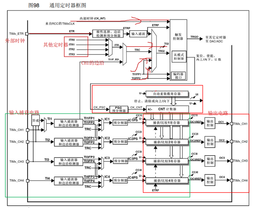
CNT Counter
The CNT counter supports up-counting mode, down-counting mode, and center-aligned mode. Down-counting mode starts from the reload value, decrements downward, and after decrementing to 0, returns to the reload value and requests an interrupt. Center-aligned mode starts from 0, first increments upward, counts to the reload value, requests an interrupt, and then decrements downward to 0, and then requests an interrupt.
Clock Source
The clock source of the general timer can not only select the internal 72MHz clock, but also the external clock.
(1)The first external clock comes fromExternal clock on TIMx_ETR pinThat is, you can connect an external square wave clock to the ETR pin of TIM2, namely PA0, and then configure the internal polarity selection, edge detection and pre-divider circuits, as well as the input filter circuit. These two circuits can perform certain shaping on the external clock. Because it is the clock of the external pin, there are inevitably some glitches, so these circuits can filter the input waveform. The filtered signal is divided into two paths. The upper ETRF enters the trigger controller, and then it can be selected as the clock of the time base unit. This path is also called "External clock mode 2”。

(2) TRGI can also provide an external clock, mainly used as a trigger input, this trigger input can trigger the slave mode of the timer. When TRGI is used as an external clock, this path is called "External clock mode 1". What are the external clocks passing through this path? The first is the signal of the ETR pin. The second is the ITR signal. This part of the clock signal comes from other timers. The TRGO of the master mode can be connected to other timers. When it is connected to other timers, it is connected to the ITR pin of other timers. ITR0 to ITR3 come from the TRGO outputs of the other four timers respectively. You can also choose TI1F_ED, which is connected to the CH1 pin of the input capture unit, that is, the clock is obtained from the CH1 pin. The suffix ED (Edge) here means edge. It can also be obtained through TI1FP1 and TI2FP2. TI1FP1 is the clock connected to the CH1 pin, and TI2FP2 is connected to the clock of the CH2 pin.
Summary: The input of external clock mode 1 can be ETR pin, other timers, edge of CH1 pin, CH1 pin and CH2 pin.
Output Comparator Circuit
The right part below is the output comparison circuit, which has four channels in total, corresponding to the pins CH1 to CH4, and can be used to output PWM waveforms to drive motors.
Input capture circuit
On the left is the input capture circuit, which also has four channels, corresponding to the CH1 to CH4 pins, which can be used to measure the frequency of the input square wave, etc.
Capture/Compare Registers
The register in the middle is the capture/compare register, which is shared by the input capture and output comparison circuits. Because input capture and output comparison cannot be used at the same time, the register and pin are shared here.
The main function:
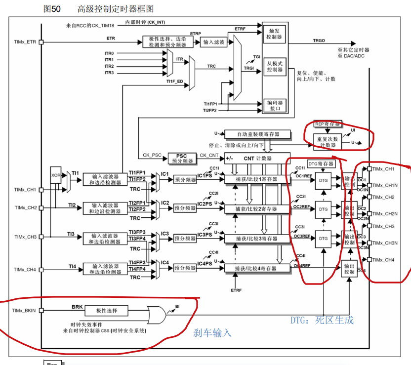
Repetition counter
The difference from the general timer is that a repetition counter is added to the interrupt request. With this counter, it is possible to achieve an update event and an update interrupt every few counting cycles. The original structure is that an update occurs after each counting cycle is completed, which is equivalent to dividing the output update signal again.
DTG Dead Zone Generator and Complementary Outputs
The following is the upgrade of the output comparison module by the advanced timer. DTG (dead time generate) is a dead zone generation circuit. The output pin on the right has been changed from one to two complementary outputs, which can output a pair of complementary PWM waves. These circuits are used to drive three-phase brushless motors, such as quadcopters, rear wheels of electric vehicles, electric drills, etc., which may all have three-phase brushless motors. Because the driving circuit of a three-phase brushless motor generally requires three bridge arms, each bridge arm is controlled by two high-power switch tubes, so a total of six high-power switch tubes are required. Therefore, the first three output PWM pins here have become complementary outputs. In addition, in order to prevent the complementary output PWM from driving the bridge arm, at the moment of switch switching, due to the imperfect device, causing a short-term direct-through phenomenon, a dead zone generation circuit is added in front. At the moment of switch switching, a dead zone of a certain length is generated, so that the upper and lower tubes of the bridge arm are all turned off to prevent the direct-through phenomenon.
Brake input
The last part is the brake input function, which is to provide safety protection for the motor drive. If the external pin BKIN (Break IN) generates a brake signal, or the internal clock fails, a fault occurs, then the control circuit will automatically cut off the motor output to prevent accidents.
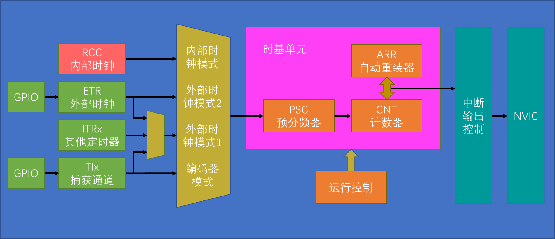
Operation control: Control some bits in the register, such as start, stop, count up or down, etc.
The right side shows where the signal goes when the timing time is up and an update interrupt is generated. If it is an advanced timer, there will be an additional repeat counter. The interrupt signal will first set an interrupt flag in the status register, and this flag will be used to apply for an interrupt to the NVIC through the interrupt output control. The interrupt output control is an interrupt output enable bit. If a certain interrupt is required, remember to enable it.


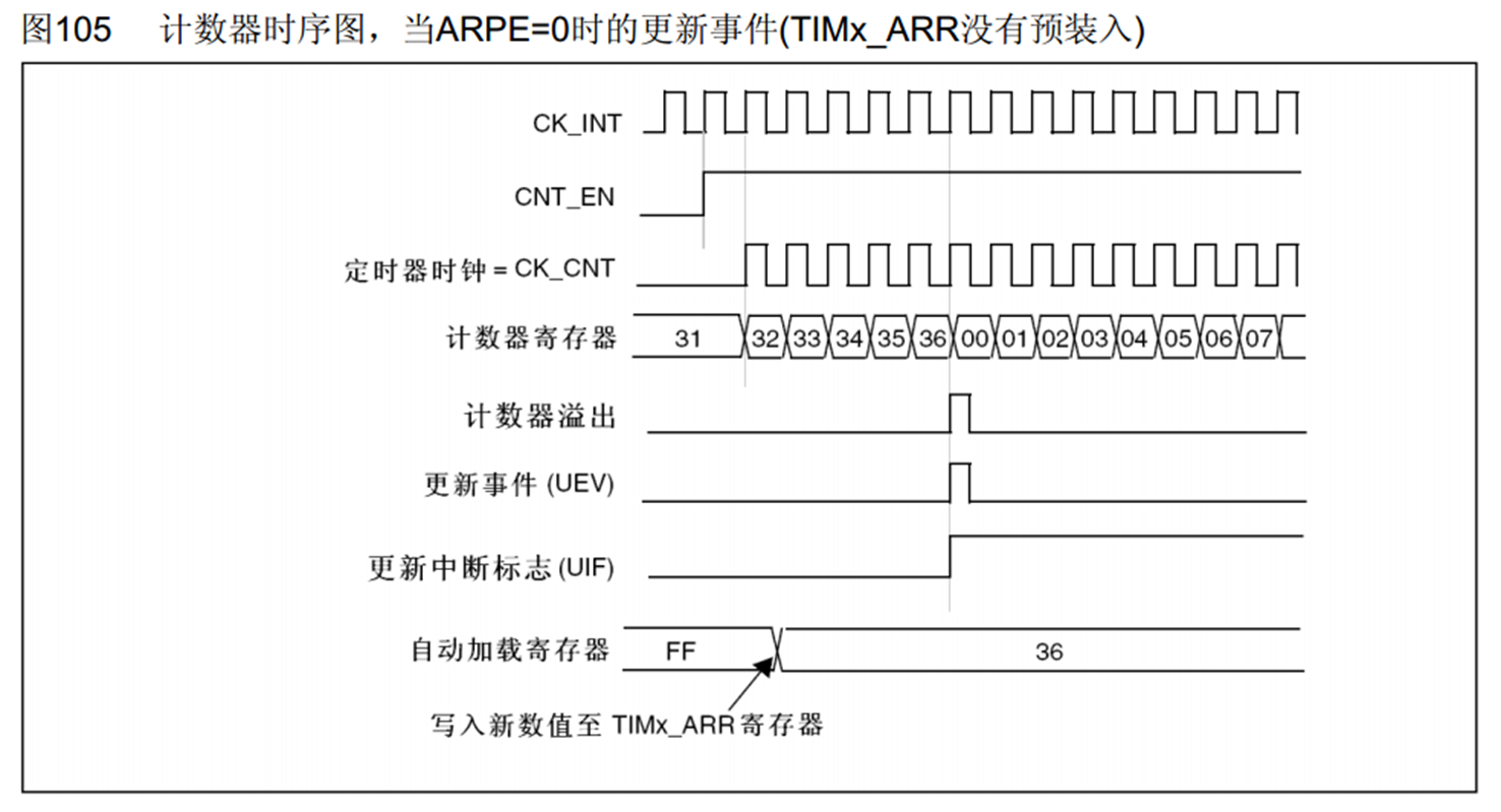
The auto-load register is changed from FF to 36, so the target value of the count value is changed from FF to 36. So after counting to 36, it will directly update and start the next round of counting.
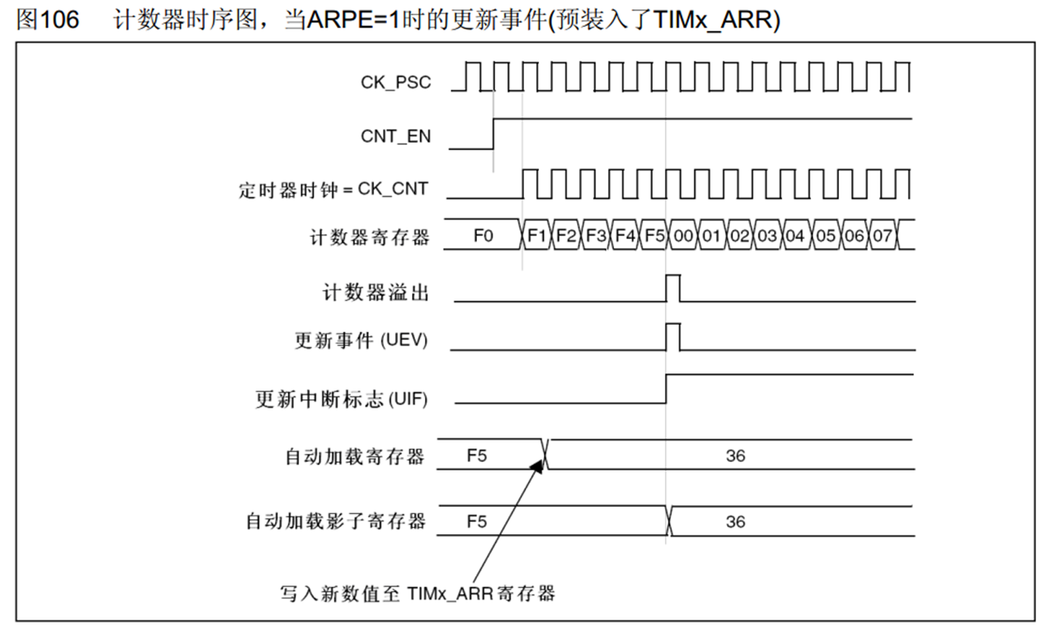
In the middle of counting, the target value of the count is changed from F5 to 36. There is a shadow register below, which is the real one. It is still F5, so the target of the count is still F5, generating an update event. At the same time, the 36 to be changed is passed to the shadow register, and the changed 36 is effective in the next counting cycle. Therefore, the purpose of introducing the shadow register is actually for synchronization, that is, to synchronize the value change with the update event to prevent errors caused by changes during operation.
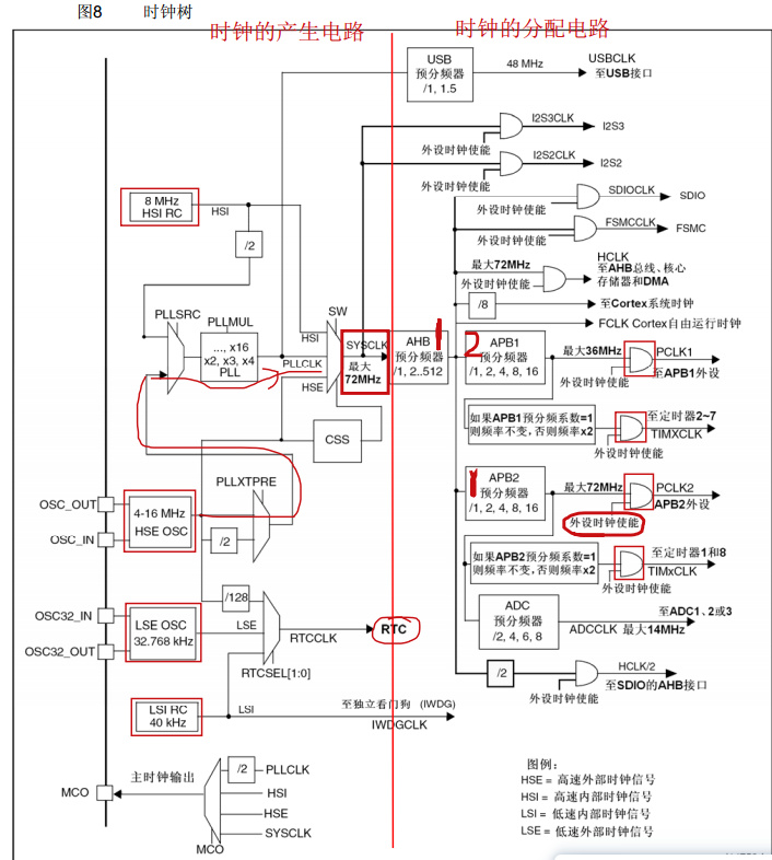
Clock Source
In the clock generation circuit, there are four oscillation sources:
(1) HSI: internal 8MHz high-speed RC oscillator;
(2) HSE: external 4~16MHz high-speed quartz crystal oscillator, also known as crystal oscillator, usually connected to 8MHz;
(3) LSE: external 32.768KHz low-speed crystal oscillator, which generally provides the clock for the RTC;
(4) LSI: Finally, there is the internal 40KHz low-speed RC oscillator, which can provide a clock for the watchdog.
The above two high-speed crystal oscillators are used to provide system clocks. The clocks of AHB, APB2, and APB1 all come from these two high-speed crystal oscillators. The only difference is that the external quartz oscillator is more stable than the internal RC oscillator, so an external crystal oscillator is generally used.
ST configuration clock
In the SystemInit function, ST configures the clock: first, it starts the internal clock HSI, selects the internal 8MHz as the system clock, and temporarily runs with the internal 8MHz clock. Then it starts the external clock, configures the external clock to enter the PLL phase-locked loop for frequency multiplication, and multiplies 8MHz by 9 times to get 72MHz. After the phase-locked loop output is stable, select the phase-locked loop output as the system clock, so that the system clock is switched from 8MHz to 72MHz.
CSS Clock Security System
CSS (clock security system): The clock security system is also responsible for switching the clock. It can monitor the operating status of the external clock. Once the external clock fails, it will automatically switch the external clock back to the internal clock to ensure the operation of the system clock and prevent accidents caused by program jams.
Clock distribution circuit
*2Then on the right, it is opened for timer 2-7 separately, because the pre-scaling coefficient here is 2, so the frequency here needs to be*2, so the clock to timer 2~7 is 72MHz. Therefore, whether it is an advanced timer, a general timer or a basic timer, their internal reference clock is 72MHz.*2Since the division factor is 1, the clocks of timers 1 and 8 are 72MHz.// 恢复缺省配置
void TIM_DeInit(TIM_TypeDef* TIMx);
// 时基单元初始化
void TIM_TimeBaseInit(TIM_TypeDef* TIMx, TIM_TimeBaseInitTypeDef* TIM_TimeBaseInitStruct);
// 结构体变量赋一个默认值
void TIM_TimeBaseStructInit(TIM_TimeBaseInitTypeDef* TIM_TimeBaseInitStruct);
// 使能计数器---运行控制
void TIM_Cmd(TIM_TypeDef* TIMx, FunctionalState NewState);
// 使能中断输出---中断输出控制
void TIM_ITConfig(TIM_TypeDef* TIMx, uint16_t TIM_IT, FunctionalState NewState);
/*-----------------时基单元的时钟选择---------*/
// 选择内部时钟
void TIM_InternalClockConfig(TIM_TypeDef* TIMx);
// 选择ITRx其他定时器的时钟
void TIM_ITRxExternalClockConfig(TIM_TypeDef* TIMx, uint16_t TIM_InputTriggerSource);
// 选择TIx捕获通道的时钟
void TIM_TIxExternalClockConfig(TIM_TypeDef* TIMx, uint16_t TIM_TIxExternalCLKSource,
uint16_t TIM_ICPolarity, uint16_t ICFilter);
// 选择ETR通过外部时钟模式1输入的时钟
void TIM_ETRClockMode1Config(TIM_TypeDef* TIMx, uint16_t TIM_ExtTRGPrescaler, uint16_t TIM_ExtTRGPolarity,
uint16_t ExtTRGFilter);
// 选择ETR通过外部时钟模式2输入的时钟
void TIM_ETRClockMode2Config(TIM_TypeDef* TIMx, uint16_t TIM_ExtTRGPrescaler,
uint16_t TIM_ExtTRGPolarity, uint16_t ExtTRGFilter);
/*--------------------------------------------------------*/
// 不是用来选择时钟的,单独用来配置ETR引脚的预分频器、极性、滤波参数的
void TIM_ETRConfig(TIM_TypeDef* TIMx, uint16_t TIM_ExtTRGPrescaler, uint16_t TIM_ExtTRGPolarity,
uint16_t ExtTRGFilter);
// 用来单独写预分频值的
void TIM_PrescalerConfig(TIM_TypeDef* TIMx, uint16_t Prescaler, uint16_t TIM_PSCReloadMode);
// 用来改变计数器的计数模式
void TIM_CounterModeConfig(TIM_TypeDef* TIMx, uint16_t TIM_CounterMode);
// 自动重装器预装功能配置
void TIM_ARRPreloadConfig(TIM_TypeDef* TIMx, FunctionalState NewState);
// 给计数器写入一个值
void TIM_SetCounter(TIM_TypeDef* TIMx, uint16_t Counter);
// 给自动重装器写入一个值
void TIM_SetAutoreload(TIM_TypeDef* TIMx, uint16_t Autoreload);
// 获取当前计数器的值
uint16_t TIM_GetCounter(TIM_TypeDef* TIMx);
// 获取当前的预分频器的值
uint16_t TIM_GetPrescaler(TIM_TypeDef* TIMx);
/*-------------获取标志位和清除标志位的------------*/
FlagStatus TIM_GetFlagStatus(TIM_TypeDef* TIMx, uint16_t TIM_FLAG);
void TIM_ClearFlag(TIM_TypeDef* TIMx, uint16_t TIM_FLAG);
ITStatus TIM_GetITStatus(TIM_TypeDef* TIMx, uint16_t TIM_IT);
void TIM_ClearITPendingBit(TIM_TypeDef* TIMx, uint16_t TIM_IT);