2024-07-12
한어Русский языкEnglishFrançaisIndonesianSanskrit日本語DeutschPortuguêsΕλληνικάespañolItalianoSuomalainenLatina
This content is based onJiangxie Technology STM32It was sorted out after learning from the video.
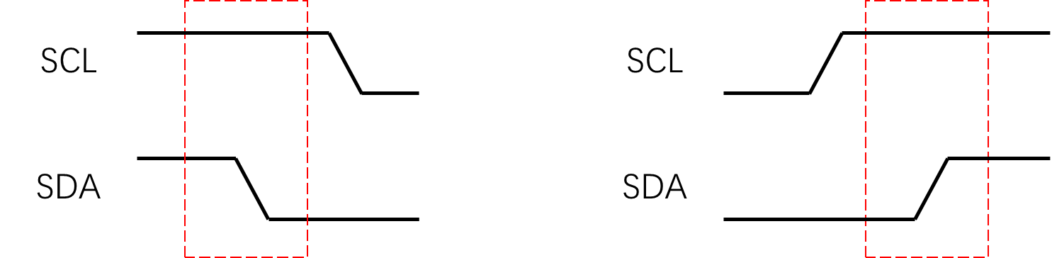
The host puts data at a low level, and reads data from the slave at a high level

After the start condition, the first byte must also be sent by the host. SCL is low, and the host wants to send 0, so it pulls SDA down to a low level; if it wants to send 1, it lets go, and SDA rebounds to a high level. During the low level of SCL, the level of SDA is allowed to change. After the data is placed, the host lets go of the clock line, and SCL rebounds to a high level. During the high level period, it is when the slave reads SDA, so during the high level period, SDA is not allowed to change. After SCL is at a high level, the slave needs to read SDA as soon as possible. Generally, the slave has completed the reading at the rising edge of SCL. Because the clock is controlled by the host, the slave does not know when the falling edge occurs, so the slave will read the data at the rising edge of SCL. When the host lets go of SCL for a period of time, it can continue to pull SCL down and transmit the next bit. The host also needs to put the data on SDA as soon as possible after the falling edge of SCL. But the host has the dominant power of the clock, so it only needs to put the data on SDA at any time of the low level. After the data is released, the host releases SCL again. When SCL is high, the slave reads this bit. This process is repeated: the host pulls SCL low and puts the data on SDA. The host releases SCL and the slave reads the SDA data. Under the synchronization of SCL, the host sends and the slave receives in turn. After 8 cycles, 8 bits of data are sent, which is a byte.
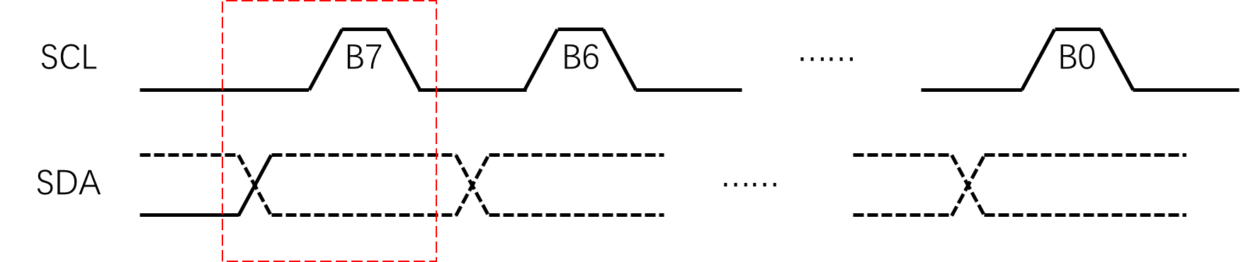
Since the high bit comes first, the first bit is the highest bit B7 of a byte, and the lowest bit B0 is sent last.
The slave device puts data at a low level, and the host device reads data at a high level
SDA line: The host must release SDA before receiving. At this time, the slave obtains the control of SDA. If the slave needs to send 0, it pulls SDA low. If the slave needs to send 1, it lets go and SDA rebounds to a high level. Low level converts data, and high level reads data. The solid line indicates the level controlled by the host, and the dotted line indicates the level controlled by the slave. SCL is controlled by the host throughout the process. The SDA host must release it before receiving and let the slave control it. Because the SCL clock is controlled by the host, the data conversion of the slave is basically carried out along the falling edge of SCL, and the host can read at any time when SCL is high.

That is, after calling the timing of sending a byte, the timing of receiving the response should be called immediately to determine whether the slave has received the data just given to it. If the slave has received it, then when the host releases SDA at the response bit, the slave should immediately pull down SDA, and then the host reads the response bit during the high level of SCL. If the response bit is 0, it means that the slave has indeed received it.
When receiving a byte, it is necessary to call the send response. The purpose of sending the response is to tell the slave whether you want to continue sending. If the slave sends a data and gets a response from the host, the slave will continue to send. If the slave does not get a response from the host, the slave will think that it has sent a data, but the host ignores it, maybe the host does not want it. At this time, the slave will obediently release SDA and hand over the control of SDA to prevent interference with the subsequent operations of the host.
process:
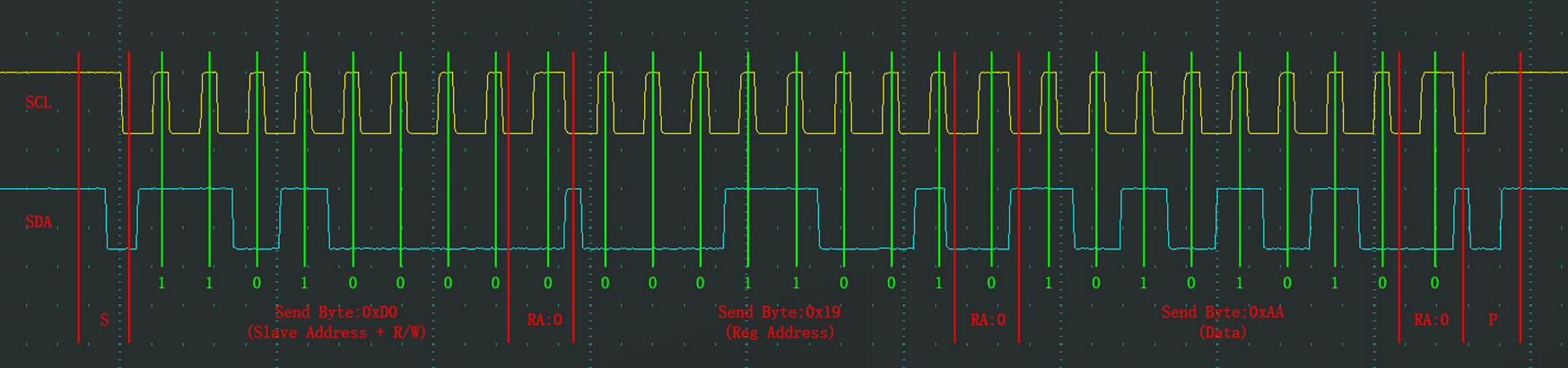
(1) Starting conditions
(2) Send a byte sequence—0xD0 (slave address (7bit) + write (1bit)-0) (1101 0000)
(3) Receive response: RA = 0 (receive response from slave)
(4) Specified address: 0x19 (0001 1001)
(5) Receive response: RA = 0 (receive response from slave)
(6) Write specified data: 0xAA (1010 1010)
(7) Receive response: RA = 0
(8) Stop bit P (termination condition)
The purpose of this data frame is to write the data 0xAA into the register at the internal address 0x19 of the device with the specified slave address 1101000.
0 means: the host will perform a write operation at the next timing;
1 means: the host will perform a read operation in the following sequence;
process:
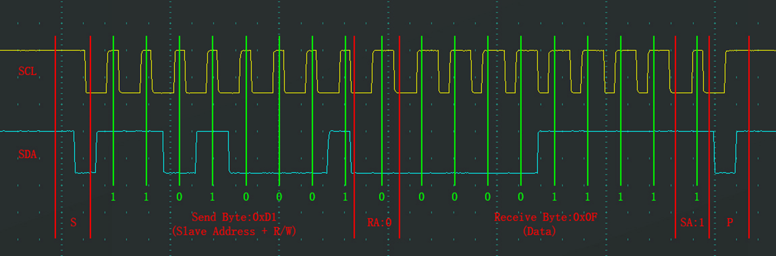
(1) Starting conditions
(2) Timing of sending a byte—0xD1 (slave address (7bit) + read (1bit)-1) (1101 0001)
(3) Receive response: RA = 0 (receive response from slave)
(4) Read slave data: 0x0F (0000 1111)
(7) Send response: SA = 0
(8) Stop bit P (termination condition)
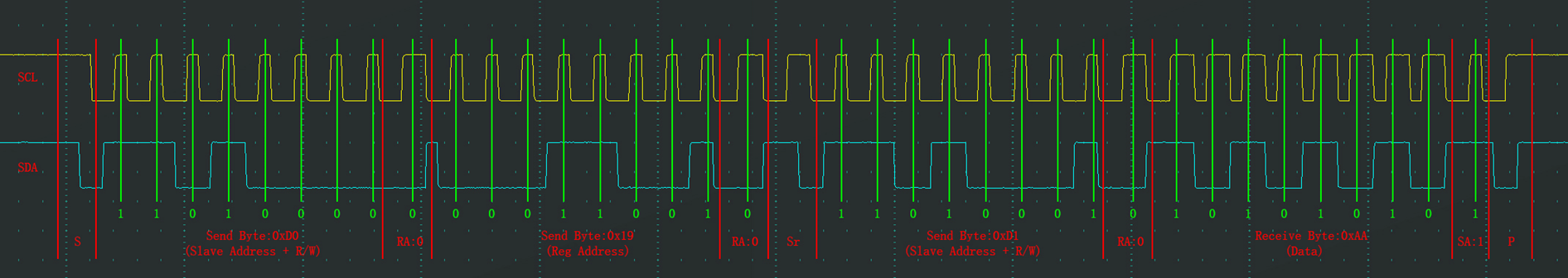
Start, repeat, then stop
process:
(1) Starting conditions
(2) Send a byte sequence—0xD0 (slave address (7bit) + write (1bit)-0) (1101 0000)
(3) Receive response: RA = 0 (receive response from slave)
(4) Specified address: 0x19 (0001 1001)
(5) Receive response: RA = 0 (receive response from slave)
(6) Repeat the start condition
(7) Timing of sending a byte—0xD1 (slave address (7bit) + read (1bit)-1) (1101 0001)
(8) Receive response: RA = 0
(9) Read slave data: 0xAA (1010 1010)
(10) Send response: SA = 0
(11) Stop bit P (termination condition)
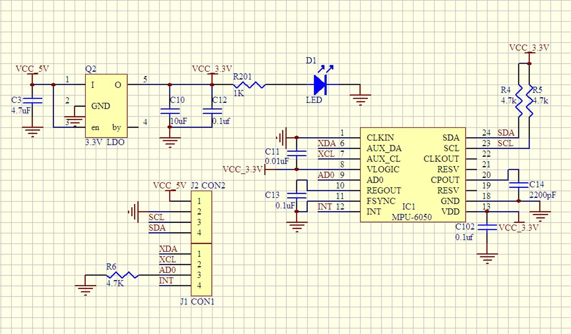
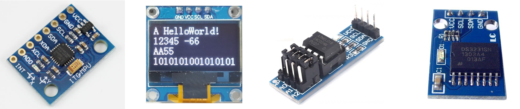
| Pinout | Function |
|---|---|
| VCC、GND | power supply |
| SCL、SDA | I2C Communication Pins |
| XCL、XDA | Host I2C communication pin |
| AD0 | The lowest bit of the slave address |
| INT | Interrupt signal output |
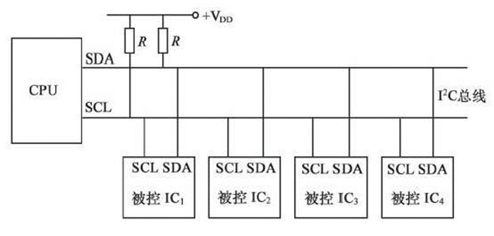
Through software I2C communication, read and write the registers inside the MPU6050 chip, write to the configuration register, and then configure the plug-in module. Read the data register to get the data of the plug-in module. The read data will be displayed on the OLED. The top data is the device ID number. The ID number of this MPU6050 is fixed to 0x68. Below, the 3 on the left are the output data of the acceleration sensor, which are the acceleration of the X-axis, Y-axis, and Z-axis, respectively. The 3 on the right are the output data of the gyroscope sensor, which are the angular velocity of the X-axis, Y-axis, and Z-axis, respectively.
SCL is connected to the PB10 pin of STM32, and SDA is connected to the PB11 pin. Since the level is flipped by software here, you can connect any two GPIO ports.
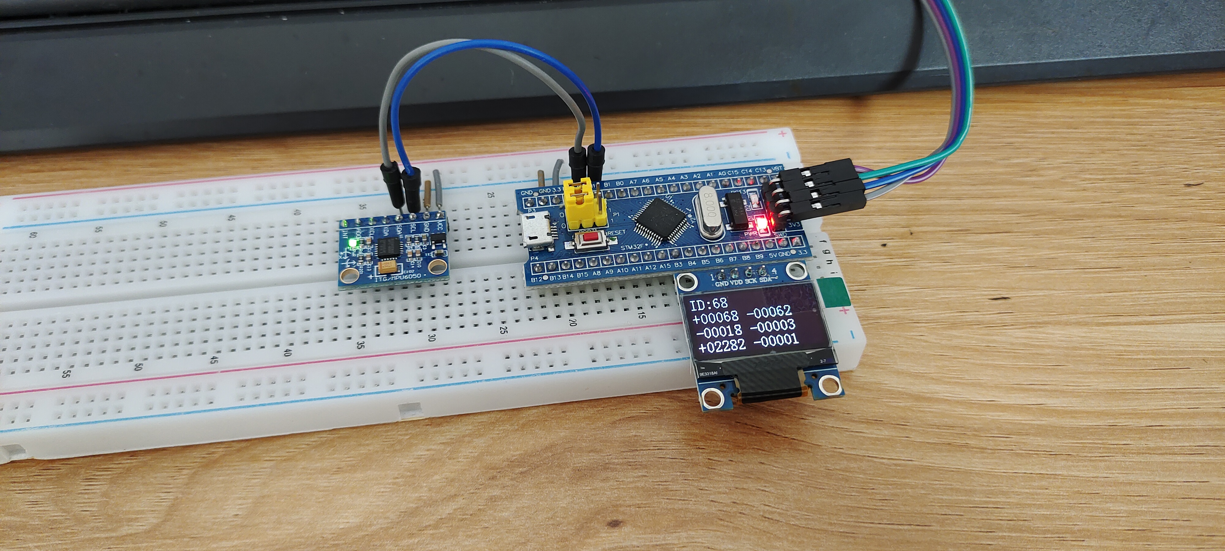
STM32 is the host and MPU6050 is the slave, which is a master-slave mode.
#include "stm32f10x.h"                  // Device header
#include "Delay.h"

void MyI2C_W_SCL(uint8_t BitValue)
{
	GPIO_WriteBit(GPIOB, GPIO_Pin_10,(BitAction)BitValue);
	Delay_us(10);
}

void MyI2C_W_SDA(uint8_t BitValue)
{
	GPIO_WriteBit(GPIOB, GPIO_Pin_11,(BitAction)BitValue);
	Delay_us(10);
}

uint8_t MyI2C_R_SDA(void)
{
	uint8_t BitValue;
	BitValue = GPIO_ReadInputDataBit(GPIOB,GPIO_Pin_11);
	Delay_us(10);
	return BitValue;
}

void MyI2C_Init(void)
{
/*
软件I2C初始化:
	1. 把SCL和SDA都初始化为开漏输出模式;
	2. 把SCL和SDA置高电平;
输入时,先输出1,再直接读取输入数据寄存器就行了;
初始化结束后,调用SetBits,把GPIOB的Pin_10和Pin_11都置高电平,
此时I2C总线处于空闲状态
*/
	RCC_APB2PeriphClockCmd(RCC_APB2Periph_GPIOB,ENABLE);
	GPIO_InitTypeDef GPIO_InitStructure;
	GPIO_InitStructure.GPIO_Mode = GPIO_Mode_Out_OD;
	GPIO_InitStructure.GPIO_Pin = GPIO_Pin_10 | GPIO_Pin_11;
	GPIO_InitStructure.GPIO_Speed = GPIO_Speed_50MHz;
	GPIO_Init(GPIOB, &GPIO_InitStructure);

	GPIO_SetBits(GPIOB, GPIO_Pin_10 | GPIO_Pin_11);

}

/*
起始条件:SCL高电平期间,SDA从高电平切换到低电平。
如果起始条件之前,SDA和SCL都已经是高电平了,那先释放哪一个是一样的效果。
但是这个Start还要兼容重复起始条件Sr,Sr最开始,SCL是低电平,SDA电平不敢确定,
所以为保险起见,在SCL低电平时,先确保释放SDA,再释放SCL。
这时SDA和SCL都是高电平,然后再拉低SDA、拉低SCL。
这样这个Start就可以兼容起始条件和重复起始条件了。
*/
void MyI2C_Start(void)
{
	MyI2C_W_SDA(1);
	MyI2C_W_SCL(1);

	MyI2C_W_SDA(0);
	MyI2C_W_SCL(0);
}

/*
终止条件:SCL高电平期间,SDA从低电平切换到高电平
如果Stop开始时,SCL和SDA都已经是低电平了,那就先释放SCL,再释放SDA。
但在这个时序单元开始时,SDA并不一定是低电平,所以为了确保之后释放
SDA能产生上升沿,要在时序单元开始时,先拉低SDA,然后再释放SCL、释放SDA。
*/
void MyI2C_Stop(void)// 终止条件
{
	MyI2C_W_SDA(0);
	MyI2C_W_SCL(1);
	MyI2C_W_SDA(1);
}

/*
发送一个字节:发送一个字节时序开始时,SCL是低电平。
除了终止条件SCL以高电平结束,所有的单元都会保证SCL以低电平结束。
SCL低电平变换数据;高电平保持数据稳定。由于是高位先行,所以变换数据的时候,
按照先放最高位,再放次高位,...,最后最低位的顺序,依次把每一个字节的每一位放在SDA线上,
每放完一位后,执行释放SCL,拉低SCL的操作,驱动时钟运转。
程序:趁SCL低电平,先把Byte的最高位放在SDA线上,
*/

void MyI2C_SendByte(uint8_t Byte) // 发送一个字节
{
	uint8_t i;
	for (i = 0; i < 8; i ++)
	{
		MyI2C_W_SDA(Byte & (0x80 >> i));// 右移i位
	    MyI2C_W_SCL(1);
	    MyI2C_W_SCL(0);
	}
}

/*
接收一个字节:时序开始时,SCL低电平,此时从机需要把数据放到SDA上,
为了防止主机干扰从机写入数据,主机需要先释放SDA,释放SDA相当于切换为输入模式,
那在SCL低电平时,从机会把数据放到SDA上,如果从机想发1,就释放SDA,想发0,就拉低SDA,
主机释放SCL,在SCL高电平期间,读取SDA,再拉低SCL,低电平期间,从机就会把下一位数据放到SDA上,重复8次,
主机就能读到一个字节了。
SCL低电平变换数据,高电平读取数据,实际上是一种读写分离的操作,低电平时间定义为写的时间,高电平时间定义为读的时间,

*/
uint8_t MyI2C_ReceiveByte(void) // 接收一个字节
{
	uint8_t i, Byte = 0x00;
	MyI2C_W_SDA(1);
	for (i = 0; i < 8; i ++)
	{
		MyI2C_W_SCL(1); // 主机读取数据
	    if (MyI2C_R_SDA() == 1) // 如果if成立,接收的这一位为1,
	    {
		    Byte |= (0x80 >> i);   // 最高位置1
	    }
        MyI2C_W_SCL(0);
	}
	return Byte;
}
/*
问题:反复读取SDA,for循环中又没写过SDA,那SDA读出来应该始终是一个值啊?
回答:I2C是在进行通信,通信是有从机的,当主机不断驱动SCL时钟时,
从机就有义务去改变SDA的电平,所以主机每次循环读取SDA的时候,
这个读取到的数据是从机控制的,这个数据也正是从机想要给我们发送的数据,
所以这个时序叫做接收一个字节。
*/

void MyI2C_SendAck(uint8_t AckBit) // 发送应答
{
	// 函数进来,SCL低电平,主机把AckBit放到SDA上,
	MyI2C_W_SDA(AckBit);
	MyI2C_W_SCL(1);  // 从机读取应答
	MyI2C_W_SCL(0);  // 进入下一个时序单元

}

uint8_t MyI2C_ReceiveAck(void) // 接收应答
{
	// 函数进来,SCL低电平,主机释放SDA,防止从机干扰
	uint8_t AckBit;
	MyI2C_W_SDA(1);  // 主机释放SDA
	MyI2C_W_SCL(1);  // SCL高电平,主机读取应答位
	AckBit = MyI2C_R_SDA();
	MyI2C_W_SCL(0);	 // SCL低电平,进入下一个时序单元
	return AckBit;
}

/*问题:在程序里,主机先把SDA置1了,然后再读取SDA,
这应答位肯定是1啊,
回答:第一,I2C的引脚是开漏输出+弱上拉的配置,主机输出1,
并不是强制SDA为高电平,而是释放SDA,
第二,I2C是在通信,主机释放了SDA,从机是有义务在此时把SDA再拉低的,
所以,即使主机把SDA置1了,之后再读取SDA,读到的值也可能是0,
读到0,代表从机给了应答,读到1,代表从机没给应答,这就是接收应答的流程。


*/
#ifndef __MPU6050_REG_H
#define __MPU6050_REG_H

// 宏定义: 寄存器的名称   对应的地址

#define	MPU6050_SMPLRT_DIV		0x19  // 采样率分频
#define	MPU6050_CONFIG			0x1A  // 配置外部帧同步(FSYNC)引脚采样和数字低通滤波器(DLPF)设置
#define	MPU6050_GYRO_CONFIG		0x1B  // 触发陀螺仪自检和配置满量程
#define	MPU6050_ACCEL_CONFIG	0x1C  // 触发加速度计自检和配置满量程

#define	MPU6050_ACCEL_XOUT_H	0x3B  // 存储最新的加速度计测量值
#define	MPU6050_ACCEL_XOUT_L	0x3C
#define	MPU6050_ACCEL_YOUT_H	0x3D
#define	MPU6050_ACCEL_YOUT_L	0x3E
#define	MPU6050_ACCEL_ZOUT_H	0x3F
#define	MPU6050_ACCEL_ZOUT_L	0x40
#define	MPU6050_TEMP_OUT_H		0x41  // 存储最新的温度传感器测量值
#define	MPU6050_TEMP_OUT_L		0x42
#define	MPU6050_GYRO_XOUT_H		0x43  // 存储最新的陀螺仪测量值
#define	MPU6050_GYRO_XOUT_L		0x44
#define	MPU6050_GYRO_YOUT_H		0x45
#define	MPU6050_GYRO_YOUT_L		0x46
#define	MPU6050_GYRO_ZOUT_H		0x47
#define	MPU6050_GYRO_ZOUT_L		0x48

#define	MPU6050_PWR_MGMT_1		0x6B  // 电源管理寄存器1
#define	MPU6050_PWR_MGMT_2		0x6C  // 电源管理寄存器2
#define	MPU6050_WHO_AM_I		0x75  // 用于验证设备身份

#endif
#include "stm32f10x.h"                  // Device header
#include "MyI2C.h"
#include "MPU6050_Reg.h"

// 宏定义:从机地址
#define MPU6050_ADDRESS  0xD0

// 指定地址写
void MPU6050_WriteReg(uint8_t RegAddress, uint8_t Data)
{
	MyI2C_Start();
	MyI2C_SendByte(MPU6050_ADDRESS);// 发送从机地址后,接收应答
	MyI2C_ReceiveAck();// 寻址找到从机之后,继续发送下一个字节
	MyI2C_SendByte(RegAddress); // 指定寄存器地址,存在MPU6050的当前地址指针里,用于指定具体读写哪个寄存器
	MyI2C_ReceiveAck();
	MyI2C_SendByte(Data);// 指定写入指定寄存器地址下的数据
	MyI2C_ReceiveAck();
	MyI2C_Stop();
}

// 指定地址读
uint8_t MPU6050_ReadReg(uint8_t RegAddress)
{
	uint8_t Data;

	MyI2C_Start();
	MyI2C_SendByte(MPU6050_ADDRESS);
	MyI2C_ReceiveAck();
	MyI2C_SendByte(RegAddress); // 指定地址:就是设置了MPU6050的当前地址指针
	MyI2C_ReceiveAck();
	// 转入读的时序,重新指定读写位,就必须重新起始
	MyI2C_Start();// 重复起始条件
	MyI2C_SendByte(MPU6050_ADDRESS | 0x01);// 指定从机地址和读写位,0xD0是写地址,或上0x01变为0xD1,读写位为1,接下来要读从机的数据
	MyI2C_ReceiveAck(); // 接收应答后,总线控制权就正式交给从机了,从机开始发送一个字节
	Data = MyI2C_ReceiveByte();// 主机接收一个字节,该函数返回值就是接收到的数据
	// 主机接收一个字节后,要给从机发送一个应答
	MyI2C_SendAck(1);// 参数为0,就是给从机应答,参数给1,就是不给从机应答
	// 如果想继续读多个字节,就要给应答,从机收到应答之后,就会继续发送数据,如果不想继续读了,就不能给从机应答了。
	// 主机收回总线的控制权,防止之后进入从机以为你还想要,但你实际不想要的冲突状态,
	// 这里,只需要读取1个字节,所以就给1,不给从机应答,
	MyI2C_Stop();
	return Data;
}

void MPU6050_Init(void)
{
	MyI2C_Init();
	// 写入一些寄存器对MPU6050硬件电路进行初始化配置
	// 电源管理寄存器1:设备复位:0,不复位;睡眠模式:0,解除睡眠:循环模式:0,不循环;无关位i:0;温度传感器失能:0,不失能;最后三位选择时钟:000,选择内部时钟,001,选择x轴的陀螺仪时钟,
	MPU6050_WriteReg(MPU6050_PWR_MGMT_1,0x01);// 解除睡眠,选择陀螺仪时钟
	// 电源管理寄存器2:前两位,循环模式唤醒频率:00,不需要;后6位,每一个轴的待机位:全为0,不需要待机;
	MPU6050_WriteReg(MPU6050_PWR_MGMT_2,0x00); // 均不待机
	// 采样率分频:该8位决定了数据输出的快慢,值越小越快
	MPU6050_WriteReg(MPU6050_SMPLRT_DIV,0x09);// 采样分频:10分频
	// 配置寄存器:外部同步:全为0,不需要;数字低通滤波器:110,最平滑的滤波
	MPU6050_WriteReg(MPU6050_CONFIG,0x06);// 滤波参数给最大
	// 陀螺仪配置寄存器:前三位,自测使能:全为0,不自测;满量程选择:11,最大量程;后三位无关位:为0
	MPU6050_WriteReg(MPU6050_GYRO_CONFIG,0x18);// 陀螺仪和加速度计都选最大量程
	// 加速度计配置寄存器:前三位,自测使能:全为0,不自测;满量程选择:11,最大量程;后三位高通滤波器:用不到,为000
	MPU6050_WriteReg(MPU6050_ACCEL_CONFIG,0x18);

}

// 获取芯片的ID号
uint8_t MPU6050_GetID(void)
{
	return MPU6050_ReadReg(MPU6050_WHO_AM_I);
}

// 获取寄存器数据的函数,返回6个int16_t的数据,分别表示XYZ的加速度值和陀螺仪值
// 指针地址传递的方法,返回多值
void MPU6050_GetData(int16_t *AccX, int16_t *AccY, int16_t *AccZ,
	                 int16_t *GyroX, int16_t *GyroY, int16_t *GyroZ)
{
	uint8_t DataH, DataL;
	// 加速度计X
	DataH = MPU6050_ReadReg(MPU6050_ACCEL_XOUT_H);
	DataL = MPU6050_ReadReg(MPU6050_ACCEL_XOUT_L);
	*AccX = (DataH << 8) | DataL; // 高8位左移8位,再或上低8位,得到加速度计X轴的16位数据
	// 加速度计Y
	DataH = MPU6050_ReadReg(MPU6050_ACCEL_YOUT_H);
	DataL = MPU6050_ReadReg(MPU6050_ACCEL_YOUT_L);
	*AccY = (DataH << 8) | DataL;
	// 加速度计Z
	DataH = MPU6050_ReadReg(MPU6050_ACCEL_ZOUT_H);
	DataL = MPU6050_ReadReg(MPU6050_ACCEL_ZOUT_L);
	*AccZ = (DataH << 8) | DataL;
	// 陀螺仪X
	DataH = MPU6050_ReadReg(MPU6050_GYRO_XOUT_H);
	DataL = MPU6050_ReadReg(MPU6050_GYRO_XOUT_L);
	*GyroX = (DataH << 8) | DataL;
	// 陀螺仪Y
	DataH = MPU6050_ReadReg(MPU6050_GYRO_YOUT_H);
	DataL = MPU6050_ReadReg(MPU6050_GYRO_YOUT_L);
	*GyroY = (DataH << 8) | DataL;
	// 陀螺仪Z
	DataH = MPU6050_ReadReg(MPU6050_GYRO_ZOUT_H);
	DataL = MPU6050_ReadReg(MPU6050_GYRO_ZOUT_L);
	*GyroZ = (DataH << 8) | DataL;
}
#include "stm32f10x.h"                  // Device header
#include "Delay.h"
#include "OLED.h"
#include "MyI2C.h"
#include "MPU6050.h"

uint8_t ID;
int16_t AX, AY, AZ, GX, GY, GZ;// 接收XYZ轴的加速度值和陀螺仪值


int main(void)
{
	OLED_Init();
//	MyI2C_Init();
	MPU6050_Init();
//
	OLED_ShowString(1,1,"ID:");
	ID = MPU6050_GetID();
	OLED_ShowHexNum(1, 4, ID, 2);

//	// 指定地址写
//	MyI2C_Start(); // 产生起始条件,开始一次传输
//	// 主机首先发送一个字节,内容是从机地址+读写位,进行寻址
//	MyI2C_SendByte(0xD0);  // 1101 000 0,0代表即将进行写入操作
//	// 发送一个字节后,要接收一下应答位,看看从机有没有收到刚才的数据
//	uint8_t Ack = MyI2C_ReceiveAck();
//	// 接收应答之后,要继续发送一个字节,写入寄存器地址
//	MyI2C_Stop();
//
//	OLED_ShowNum(1, 1, Ack, 3);

//	// 指定地址读
//	uint8_t ID = MPU6050_ReadReg(0X75);// 返回值是0x68
//	OLED_ShowHexNum(1, 1, ID, 2);

//	// 指定地址写,需要先解除睡眠模式,否则写入无效
//	// 睡眠模式是电源管理寄存器1的这一位SLEEP控制的,把该寄存器写入0x00,解除睡眠模式
//	// 该寄存器地址是0x6B
//	MPU6050_WriteReg(0x6B, 0x00);
//	// 采样率分频寄存器,地址是0x19,值的内容是采样分频
//	MPU6050_WriteReg(0x19, 0xAA);
//
//	uint8_t ID = MPU6050_ReadReg(0X19);
//	OLED_ShowHexNum(1, 1, ID, 2);//显示0x19地址下的内容,应该是0xAA

	while(1)
	{
		MPU6050_GetData(&AX, &AY, &AZ, &GX, &GY, &GZ);
		OLED_ShowSignedNum(2, 1, AX, 5);
		OLED_ShowSignedNum(3, 1, AY, 5);
		OLED_ShowSignedNum(4, 1, AZ, 5);
		OLED_ShowSignedNum(2, 8, GX, 5);
		OLED_ShowSignedNum(3, 8, GY, 5);
		OLED_ShowSignedNum(4, 8, GZ, 5);
	}
}
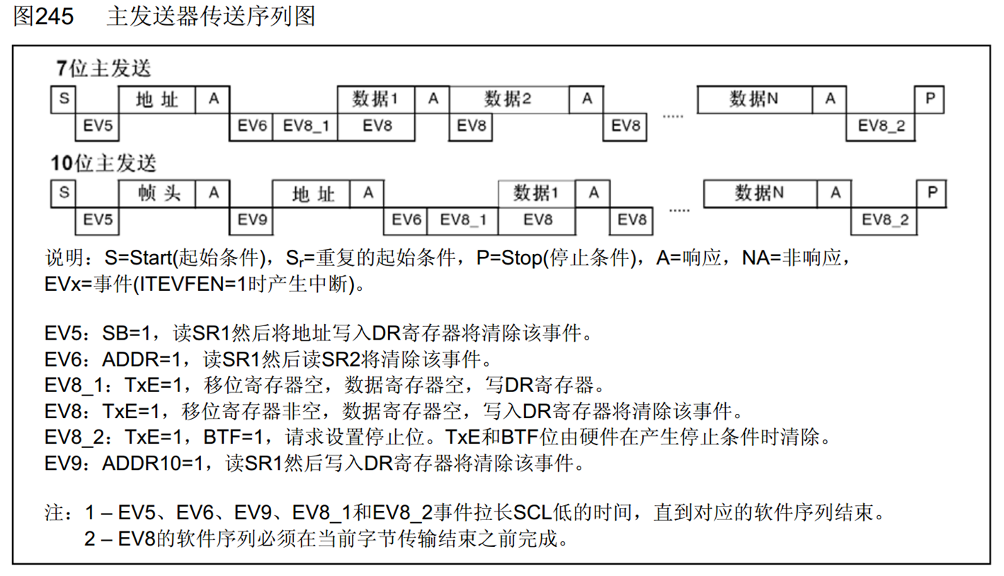
When the STM32 wants to execute a write to a specified address, it needs to follow the transmitter transmission sequence diagram.
7-bit master reception: start, slave address + read, receive response, receive data, send response... receive data, non-response, stop
void I2C_DeInit(I2C_TypeDef* I2Cx);
void I2C_Init(I2C_TypeDef* I2Cx, I2C_InitTypeDef* I2C_InitStruct);
void I2C_StructInit(I2C_InitTypeDef* I2C_InitStruct);
void I2C_Cmd(I2C_TypeDef* I2Cx, FunctionalState NewState);
// 生成起始条件、终止条件
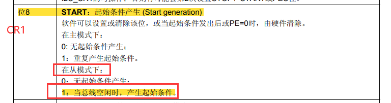
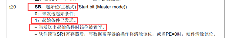
void I2C_GenerateSTART(I2C_TypeDef* I2Cx, FunctionalState NewState);
void I2C_GenerateSTOP(I2C_TypeDef* I2Cx, FunctionalState NewState);
// 配置CR1的ACK这一位,0:无应答,1:应答
void I2C_AcknowledgeConfig(I2C_TypeDef* I2Cx, FunctionalState NewState);
// 发送数据,把Data数据直接写入到DR寄存器
void I2C_SendData(I2C_TypeDef* I2Cx, uint8_t Data);
// 读取DR,接收数据
uint8_t I2C_ReceiveData(I2C_TypeDef* I2Cx);
// Address参数也是通过DR发送的,但在发送之前,设置了Address最低位的读写位,
// I2C_Direction不是发送,是把Address的最低位置1(读),否则最低位清0(写)
void I2C_Send7bitAddress(I2C_TypeDef* I2Cx, uint8_t Address, uint8_t I2C_Direction);
SCL is connected to the PB10 pin of STM32, and SDA is connected to the PB11 pin. Since the level is flipped by software here, you can connect any two GPIO ports.
The data on the top of the OLED is the device ID number, and the ID number of this MPU6050 is fixed to 0x68. Below, the 3 on the left are the output data of the acceleration sensor, which are the acceleration of the X-axis, Y-axis, and Z-axis, and the 3 on the right are the output data of the gyroscope sensor, which are the angular velocity of the X-axis, Y-axis, and Z-axis.
#include "stm32f10x.h" // Device header
#include "MPU6050_Reg.h"
/*
1. 配置I2C外设,对I2C外设进行初始化,替换MyI2C_Init
(1)开启I2C外设和对应GPIO口的时钟,
(2)把I2C外设对应的GPIO口初始化为复用开漏模式
(3)使用结构体,对整个I2C进行配置
(4)I2C_Cmd,使能I2C
2. 控制外设电路,实现指定地址写的时序,替换WriteReg
3. 控制外设电路,实现指定地址读的时序,替换ReadReg
*/
// 宏定义:从机地址
#define MPU6050_ADDRESS 0xD0
// 超时退出
void MPU6050_WaitEvent(I2C_TypeDef* I2Cx, uint32_t I2C_EVENT)
{
uint32_t TimeOut;
TimeOut = 10000;
while (I2C_CheckEvent(I2Cx, I2C_EVENT) != SUCCESS)
{
TimeOut --;
if (TimeOut == 0)
{
break;// 跳出循环,直接执行后面的程序
}
}
}
// 指定地址写:发送器传送时序
void MPU6050_WriteReg(uint8_t RegAddress, uint8_t Data)
{
// MyI2C_Start();
// MyI2C_SendByte(MPU6050_ADDRESS);// 发送从机地址后,接收应答
// MyI2C_ReceiveAck();// 寻址找到从机之后,继续发送下一个字节
// MyI2C_SendByte(RegAddress); // 指定寄存器地址,存在MPU6050的当前地址指针里,用于指定具体读写哪个寄存器
// MyI2C_ReceiveAck();
// MyI2C_SendByte(Data);// 指定写入指定寄存器地址下的数据
// MyI2C_ReceiveAck();
// MyI2C_Stop();
I2C_GenerateSTART(I2C2, ENABLE); // 起始条件
MPU6050_WaitEvent(I2C2, I2C_EVENT_MASTER_MODE_SELECT); //EV5事件
// 发送从机地址,接收应答。该函数自带了接收应答,如果应答错误,硬件会通过标志位和中断来提示我们
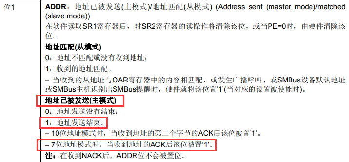
I2C_Send7bitAddress(I2C2, MPU6050_ADDRESS, I2C_Direction_Transmitter);
MPU6050_WaitEvent(I2C2, I2C_EVENT_MASTER_TRANSMITTER_MODE_SELECTED); //EV6事件
// 直接写入DR,发送数据
I2C_SendData(I2C2, RegAddress);
// 写入了DR,DR立刻转移到移位寄存器进行发送,EV8事件出现的非常快,基本不用等。因为有两级缓存,
// 第一个数据写进DR了,会立刻跑到移位寄存器,这时不用等第一个数据发完,第二个数据就可以写进去等着了。
MPU6050_WaitEvent(I2C2, I2C_EVENT_MASTER_BYTE_TRANSMITTING); //EV8事件
I2C_SendData(I2C2, Data);
MPU6050_WaitEvent(I2C2, I2C_EVENT_MASTER_BYTE_TRANSMITTED); //EV8_2事件
I2C_GenerateSTOP(I2C2, ENABLE);
}
// 指定地址读:接收器传送序列
uint8_t MPU6050_ReadReg(uint8_t RegAddress)
{
uint8_t Data;
// MyI2C_Start();
// MyI2C_SendByte(MPU6050_ADDRESS);
// MyI2C_ReceiveAck();
// MyI2C_SendByte(RegAddress); // 指定地址:就是设置了MPU6050的当前地址指针
// MyI2C_ReceiveAck();
// // 转入读的时序,重新指定读写位,就必须重新起始
// MyI2C_Start();// 重复起始条件
// MyI2C_SendByte(MPU6050_ADDRESS | 0x01);// 指定从机地址和读写位,0xD0是写地址,或上0x01变为0xD1,读写位为1,接下来要读从机的数据
// MyI2C_ReceiveAck(); // 接收应答后,总线控制权就正式交给从机了,从机开始发送一个字节
// Data = MyI2C_ReceiveByte();// 主机接收一个字节,该函数返回值就是接收到的数据
// // 主机接收一个字节后,要给发送从机一个应答
// MyI2C_SendAck(1);// 参数为0,就是给从机应答,参数给1,就是不给从机应答
// MyI2C_Stop();
I2C_GenerateSTART(I2C2, ENABLE); // 起始条件
MPU6050_WaitEvent(I2C2, I2C_EVENT_MASTER_MODE_SELECT); //EV5事件
// 发送从机地址,接收应答。该函数自带了接收应答,如果应答错误,硬件会通过标志位和中断来提示我们
I2C_Send7bitAddress(I2C2, MPU6050_ADDRESS, I2C_Direction_Transmitter);
MPU6050_WaitEvent(I2C2, I2C_EVENT_MASTER_TRANSMITTER_MODE_SELECTED); //EV6事件
// 直接写入DR,发送数据
I2C_SendData(I2C2, RegAddress);
// 写入了DR,DR立刻转移到移位寄存器进行发送,EV8事件出现的非常快,基本不用等。因为有两级缓存,
// 第一个数据写进DR了,会立刻跑到移位寄存器,这时不用等第一个数据发完,第二个数据就可以写进去等着了。
MPU6050_WaitEvent(I2C2, I2C_EVENT_MASTER_BYTE_TRANSMITTED); //EV8_2事件
I2C_GenerateSTART(I2C2, ENABLE);// 重复起始条件
// 主机接收
MPU6050_WaitEvent(I2C2, I2C_EVENT_MASTER_MODE_SELECT); //EV5事件
// 接收地址
I2C_Send7bitAddress(I2C2, MPU6050_ADDRESS, I2C_Direction_Receiver); // 函数内部就自动将该地址MPU6050_ADDRESS的最低位置1
MPU6050_WaitEvent(I2C2, I2C_EVENT_MASTER_RECEIVER_MODE_SELECTED); //EV6事件
// 在最后一个数据之前就要把应答位ACK置0,同时把停止条件生成位STOP置1
I2C_AcknowledgeConfig(I2C2, DISABLE);
I2C_GenerateSTOP(I2C2, ENABLE);
MPU6050_WaitEvent(I2C2, I2C_EVENT_MASTER_BYTE_RECEIVED); //EV7事件
// 等EV7事件产生后,一个字节的数据就已经在DR里面了。
// 读取DR就可拿出该字节
Data = I2C_ReceiveData(I2C2); // 返回值就是DR的数据
// 在接收函数的最后,要恢复默认的ACK = 1。
// 默认状态下ACK就是1,给从机应答,在收最后一个字节之前,临时把ACK置0,给非应答,
// 所以在接收函数的最后,要恢复默认的ACK = 1,这个流程是为了方便指定地址收多个字节。
I2C_AcknowledgeConfig(I2C2, ENABLE);
return Data;
}
void MPU6050_Init(void)
{
// MyI2C_Init();
RCC_APB1PeriphClockCmd(RCC_APB1Periph_I2C2, ENABLE);
RCC_APB2PeriphClockCmd(RCC_APB2Periph_GPIOB,ENABLE);
GPIO_InitTypeDef GPIO_InitStructure;
GPIO_InitStructure.GPIO_Mode = GPIO_Mode_AF_OD; // 复用开漏
GPIO_InitStructure.GPIO_Pin = GPIO_Pin_10 | GPIO_Pin_11;
GPIO_InitStructure.GPIO_Speed = GPIO_Speed_50MHz;
GPIO_Init(GPIOB, &GPIO_InitStructure);
I2C_InitTypeDef I2C_InitStructure;
I2C_InitStructure.I2C_Mode = I2C_Mode_I2C; // 模式
I2C_InitStructure.I2C_ClockSpeed = 50000; // 时钟速度,最大400kHz的时钟频率
I2C_InitStructure.I2C_DutyCycle = I2C_DutyCycle_2; // 时钟占空比,只有在时钟频率大于100kHz,也就是进入到快速状态时才有用,小于100kHz,占空比是固定的1:1,
I2C_InitStructure.I2C_Ack = I2C_Ack_Enable; //
I2C_InitStructure.I2C_AcknowledgedAddress = I2C_AcknowledgedAddress_7bit; // STM32作为从机,可以响应几位的地址
I2C_InitStructure.I2C_OwnAddress1 = 0x00; // 自身地址1,也是作为从机使用,
I2C_Init(I2C2, &I2C_InitStructure);
I2C_Cmd(I2C2,ENABLE);
// 写入一些寄存器对MPU6050硬件电路进行初始化配置
// 电源管理寄存器1:设备复位:0,不复位;睡眠模式:0,解除睡眠:循环模式:0,不循环;无关位i:0;温度传感器失能:0,不失能;最后三位选择时钟:000,选择内部时钟,001,选择x轴的陀螺仪时钟,
MPU6050_WriteReg(MPU6050_PWR_MGMT_1,0x01);// 解除睡眠,选择陀螺仪时钟
// 电源管理寄存器2:前两位,循环模式唤醒频率:00,不需要;后6位,每一个轴的待机位:全为0,不需要待机;
MPU6050_WriteReg(MPU6050_PWR_MGMT_2,0x00); // 均不待机
// 采样率分频:该8位决定了数据输出的快慢,值越小越快
MPU6050_WriteReg(MPU6050_SMPLRT_DIV,0x09);// 采样分频:10分频
// 配置寄存器:外部同步:全为0,不需要;数字低通滤波器:110,最平滑的滤波
MPU6050_WriteReg(MPU6050_CONFIG,0x06);// 滤波参数给最大
// 陀螺仪配置寄存器:前三位,自测使能:全为0,不自测;满量程选择:11,最大量程;后三位无关位:为0
MPU6050_WriteReg(MPU6050_GYRO_CONFIG,0x18);// 陀螺仪和加速度计都选最大量程
// 加速度计配置寄存器:前三位,自测使能:全为0,不自测;满量程选择:11,最大量程;后三位高通滤波器:用不到,为000
MPU6050_WriteReg(MPU6050_ACCEL_CONFIG,0x18);
}
// 获取芯片的ID号
uint8_t MPU6050_GetID(void)
{
return MPU6050_ReadReg(MPU6050_WHO_AM_I);
}
// 获取寄存器数据的函数,返回6个int16_t的数据,分别表示XYZ的加速度值和陀螺仪值
// 指针地址传递的方法,返回多值
void MPU6050_GetData(int16_t *AccX, int16_t *AccY, int16_t *AccZ,
int16_t *GyroX, int16_t *GyroY, int16_t *GyroZ)
{
uint8_t DataH, DataL;
// 加速度计X
DataH = MPU6050_ReadReg(MPU6050_ACCEL_XOUT_H);
DataL = MPU6050_ReadReg(MPU6050_ACCEL_XOUT_L);
*AccX = (DataH << 8) | DataL; // 高8位左移8位,再或上低8位,得到加速度计X轴的16位数据
// 加速度计Y
DataH = MPU6050_ReadReg(MPU6050_ACCEL_YOUT_H);
DataL = MPU6050_ReadReg(MPU6050_ACCEL_YOUT_L);
*AccY = (DataH << 8) | DataL;
// 加速度计Z
DataH = MPU6050_ReadReg(MPU6050_ACCEL_ZOUT_H);
DataL = MPU6050_ReadReg(MPU6050_ACCEL_ZOUT_L);
*AccZ = (DataH << 8) | DataL;
// 陀螺仪X
DataH = MPU6050_ReadReg(MPU6050_GYRO_XOUT_H);
DataL = MPU6050_ReadReg(MPU6050_GYRO_XOUT_L);
*GyroX = (DataH << 8) | DataL;
// 陀螺仪Y
DataH = MPU6050_ReadReg(MPU6050_GYRO_YOUT_H);
DataL = MPU6050_ReadReg(MPU6050_GYRO_YOUT_L);
*GyroY = (DataH << 8) | DataL;
// 陀螺仪Z
DataH = MPU6050_ReadReg(MPU6050_GYRO_ZOUT_H);
DataL = MPU6050_ReadReg(MPU6050_GYRO_ZOUT_L);
*GyroZ = (DataH << 8) | DataL;
}
#include "stm32f10x.h"                  // Device header
#include "Delay.h"
#include "OLED.h"
#include "MPU6050.h"

uint8_t ID;
int16_t AX, AY, AZ, GX, GY, GZ;// 接收XYZ轴的加速度值和陀螺仪值


int main(void)
{
	OLED_Init();
	MPU6050_Init();

	OLED_ShowString(1,1,"ID:");
	ID = MPU6050_GetID();
	OLED_ShowHexNum(1, 4, ID, 2);

//	// 指定地址写
//	MyI2C_Start(); // 产生起始条件,开始一次传输
//	// 主机首先发送一个字节,内容时从机地址+读写位,进行寻址
//	MyI2C_SendByte(0xD0);  // 1101 000 0,0代表即将进行写入操作
//	// 发送一个字节后,要接收一下应答位,看看从机有没有收到刚才的数据
//	uint8_t Ack = MyI2C_ReceiveAck();
//	// 接收应答之后,要继续发送一个字节,写入寄存器地址
//	MyI2C_Stop();
//
//	OLED_ShowNum(1, 1, Ack, 3);

//	// 指定地址读
//	uint8_t ID = MPU6050_ReadReg(0X75);// 返回值是0x68
//	OLED_ShowHexNum(1, 1, ID, 2);

//	// 指定地址写,需要先解除睡眠模式,否则写入无效
//	// 睡眠模式是电源管理寄存器1的这一位SLEEP控制的,把该寄存器写入0x00,解除睡眠模式
//	// 该寄存器地址是0x6B
//	MPU6050_WriteReg(0x6B, 0x00);
//	// 采样率分频寄存器,地址是0x19,值的内容是采样分频
//	MPU6050_WriteReg(0x19, 0xAA);
//
//	uint8_t ID = MPU6050_ReadReg(0X19);
//	OLED_ShowHexNum(1, 1, ID, 2);//显示0x19地址下的内容,应该是0xAA


	while(1)
	{
		MPU6050_GetData(&AX, &AY, &AZ, &GX, &GY, &GZ);
		OLED_ShowSignedNum(2, 1, AX, 5);
		OLED_ShowSignedNum(3, 1, AY, 5);
		OLED_ShowSignedNum(4, 1, AZ, 5);
		OLED_ShowSignedNum(2, 8, GX, 5);
		OLED_ShowSignedNum(3, 8, GY, 5);
		OLED_ShowSignedNum(4, 8, GZ, 5);
	}
}

I have devoted myself to the research of technology for more than 30 years. I am proficient in various languages such as Java, Linux, JavaScript, PHP, CSS, etc. I have made many contributions in the field of open source. I have established a developer documentation site to share some problems in technology development for everyone to read.