2024-07-12
한어Русский языкEnglishFrançaisIndonesianSanskrit日本語DeutschPortuguêsΕλληνικάespañolItalianoSuomalainenLatina
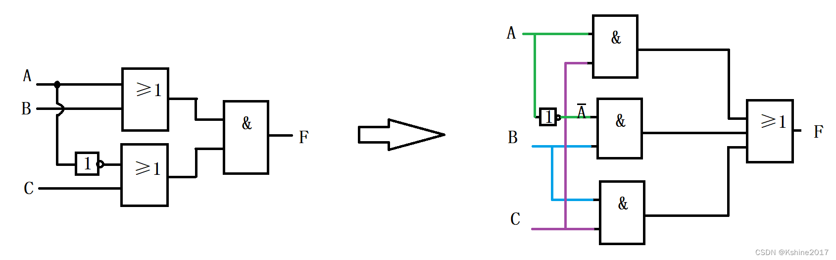
(1) As shown in the figure below.
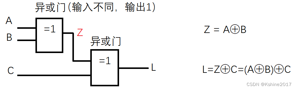
(2) List the truth table
| A | B | C | Z | L |
|---|---|---|---|---|
| 0 | 0 | 0 | 0 | 0 |
| 0 | 0 | 1 | 0 | 1 |
| 0 | 1 | 0 | 1 | 1 |
| 0 | 1 | 1 | 1 | 0 |
| 1 | 0 | 0 | 1 | 1 |
| 1 | 0 | 1 | 1 | 0 |
| 1 | 1 | 0 | 0 | 0 |
| 1 | 1 | 1 | 0 | 1 |
(3) AnalyzeOdd parity circuitFunction.
(1) Based on the odd-parity circuit, adding an inverter at the output end can obtainEven parity circuit。
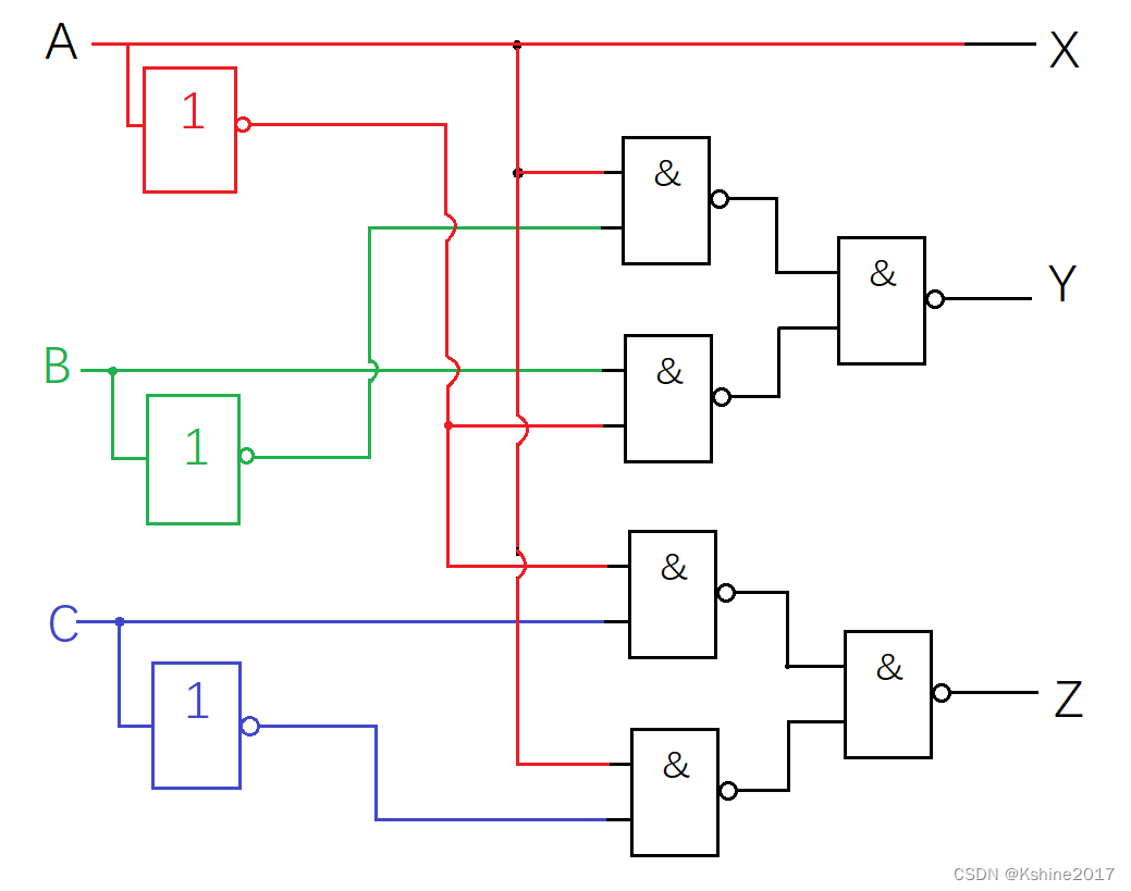
| A | B | C | X | Y | Z |
|---|---|---|---|---|---|
| 0 | 0 | 0 | 0 | 0 | 0 |
| 0 | 0 | 1 | 0 | 0 | 1 |
| 0 | 1 | 0 | 0 | 1 | 0 |
| 0 | 1 | 1 | 0 | 1 | 1 |
| 1 | 0 | 0 | 1 | 1 | 1 |
| 1 | 0 | 1 | 1 | 1 | 0 |
| 1 | 1 | 0 | 1 | 0 | 1 |
| 1 | 1 | 1 | 1 | 0 | 0 |
need.
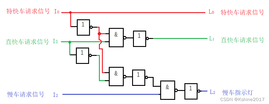
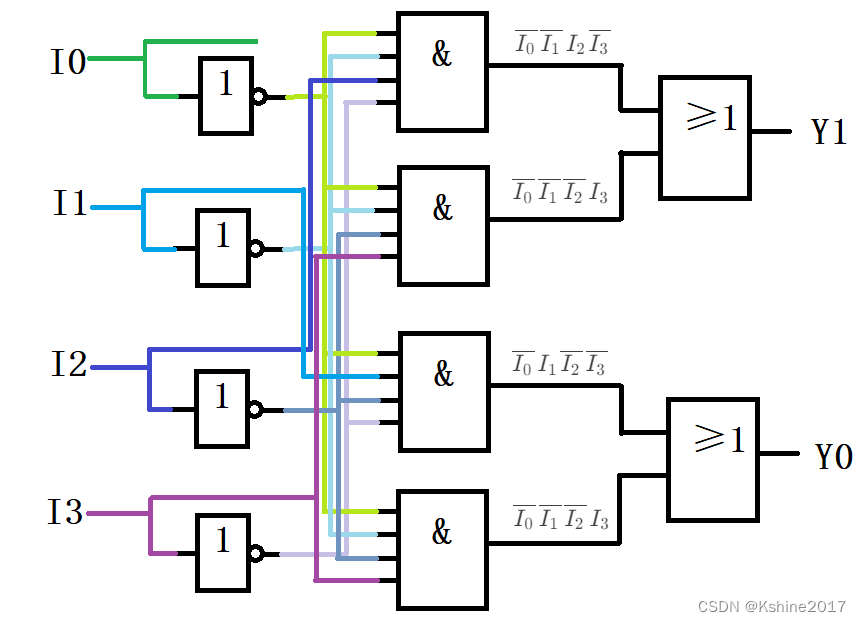
(1) Using 2 inputsNAND Gate,inverter.
(2) Indicator light No. 1, the indicator light for express trains entering the station. It has a high priority.
(3) Indicator light No. 2, the indicator light for express trains entering the station. Medium priority.
(4) Indicator light No. 3, slow train approaching station indicator light. Low priority.
(5) Only one indicator light can be on at a time.
Define input and output variables.
(1) Input signal, I 0 Express request, I 1 Direct express request, I 2 Slow train request I_0 Express request, I_1 Direct express request, I_2 Slow train requestI0Express request,I1Please ask immediately.I2Slow train request1 means there is a request to enter the station, and 0 means there is no request to enter the station.
(2) Output signal, L 0 Express station indicator, L 1 Direct express station indicator, L 2 Slow train station indicator L_0 Express station indicator, L_1 Direct express station indicator, L_2 Slow train station indicatorL0Express arrival indicator light,L1Fast-track indicator light,L2Slow train approaching station indicator1 means the light is on, 0 means the light is off.
Truth table.
| enter | Output | ||||
| I_0 | I_1 | I_2 | L_0 | L_1 | L_2 |
| 0 | 0 | 0 | 0 | 0 | 0 |
| 1 | X | X | 1 | 0 | 0 |
| 0 | 1 | X | 0 | 1 | 0 |
| 0 | 0 | 1 | 0 | 0 | 1 |
List logical expressions
L
0
=
I
0
L_0 = I_0
L0=I0
L
1
=
I
0
‾
⋅
I
1
L_1 = overline{I_0}·I_1
L1=I0⋅I1
L
2
=
I
0
‾
⋅
I
1
‾
⋅
I
2
L_2 = overline{I_0}·overline{I_1}·I_2
L2=I0⋅I1⋅I2
Transform to the AND-NOT form as required.
L
0
=
I
0
L_0 = I_0
L0=I0
L
1
=
I
0
‾
⋅
I
1
‾
‾
L_1 = overline{overline{overline{I_0}·I_1}}
L1=I0⋅I1
L
2
=
I
0
‾
⋅
I
1
‾
‾
‾
⋅
I
2
‾
‾
L_2 =overline{overline{overline{overline{overline{I_0}·overline{I_1}}}·I_2}}
L2=I0⋅I1⋅I2
Draw a logic diagram.
(1) A 74HC00 chip, containing four 2-input CMOS NAND gates.
(2) A 74HC04 chip contains 6 CMOS inverters.
need.
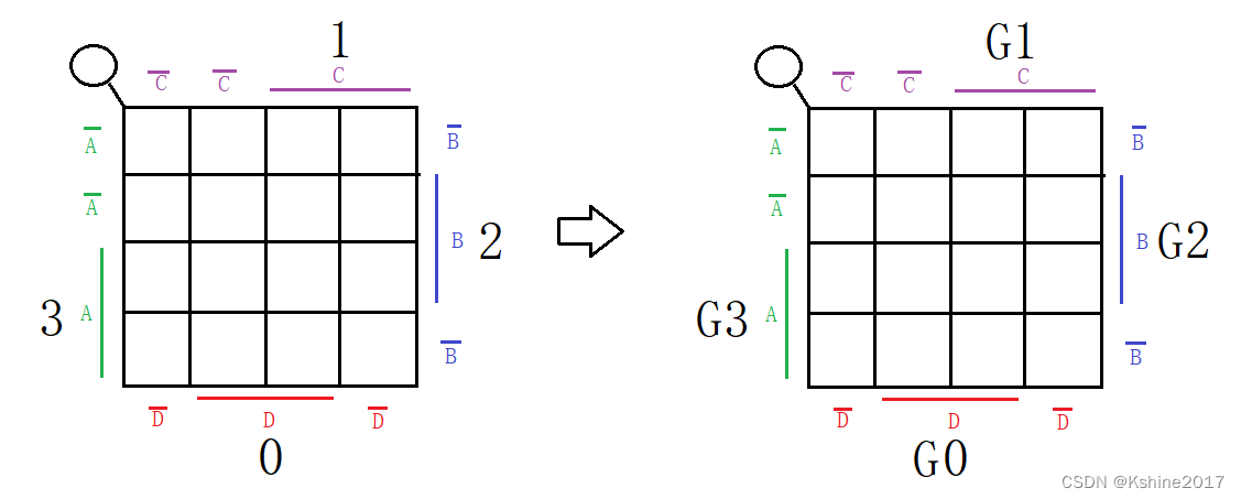
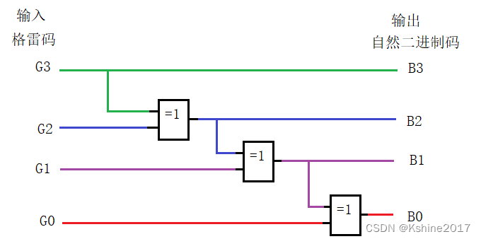
(1) Any logic gate circuit can be used.
(2) 4-bit Gray code, converted to natural binary code.
Define input and output variables.
(1) Input variables,
G
3
,
G
2
,
G
1
,
G
0
G_3,G_2,G_1,G_0
G3,G2,G1,G0。
(2) Output variables,
B
3
,
B
2
,
B
1
,
B
0
B_3,B_2,B_1,B_0
B3,B2,B1,B0。
List the truth table.
| enter | Output | ||||||
| G_3 | G_2 | G_1 | G_0 | B_3 | B_2 | B_1 | B_0 |
| 0 | 0 | 0 | 0 | 0 | 0 | 0 | 0 |
| 0 | 0 | 0 | 1 | 0 | 0 | 0 | 1 |
| 0 | 0 | 1 | 1 | 0 | 0 | 1 | 0 |
| 0 | 0 | 1 | 0 | 0 | 0 | 1 | 1 |
| 0 | 1 | 1 | 0 | 0 | 1 | 0 | 0 |
| 0 | 1 | 1 | 1 | 0 | 1 | 0 | 1 |
| 0 | 1 | 0 | 1 | 0 | 1 | 1 | 0 |
| 0 | 1 | 0 | 0 | 0 | 1 | 1 | 1 |
| 1 | 1 | 0 | 0 | 1 | 0 | 0 | 0 |
| 1 | 1 | 0 | 1 | 1 | 0 | 0 | 1 |
| 1 | 1 | 1 | 1 | 1 | 0 | 1 | 0 |
| 1 | 1 | 1 | 0 | 1 | 0 | 1 | 1 |
| 1 | 0 | 1 | 0 | 1 | 1 | 0 | 0 |
| 1 | 0 | 1 | 1 | 1 | 1 | 0 | 1 |
| 1 | 0 | 0 | 1 | 1 | 1 | 1 | 0 |
| 1 | 0 | 0 | 0 | 1 | 1 | 1 | 1 |
Based on the truth table, draw the Karnaugh map.
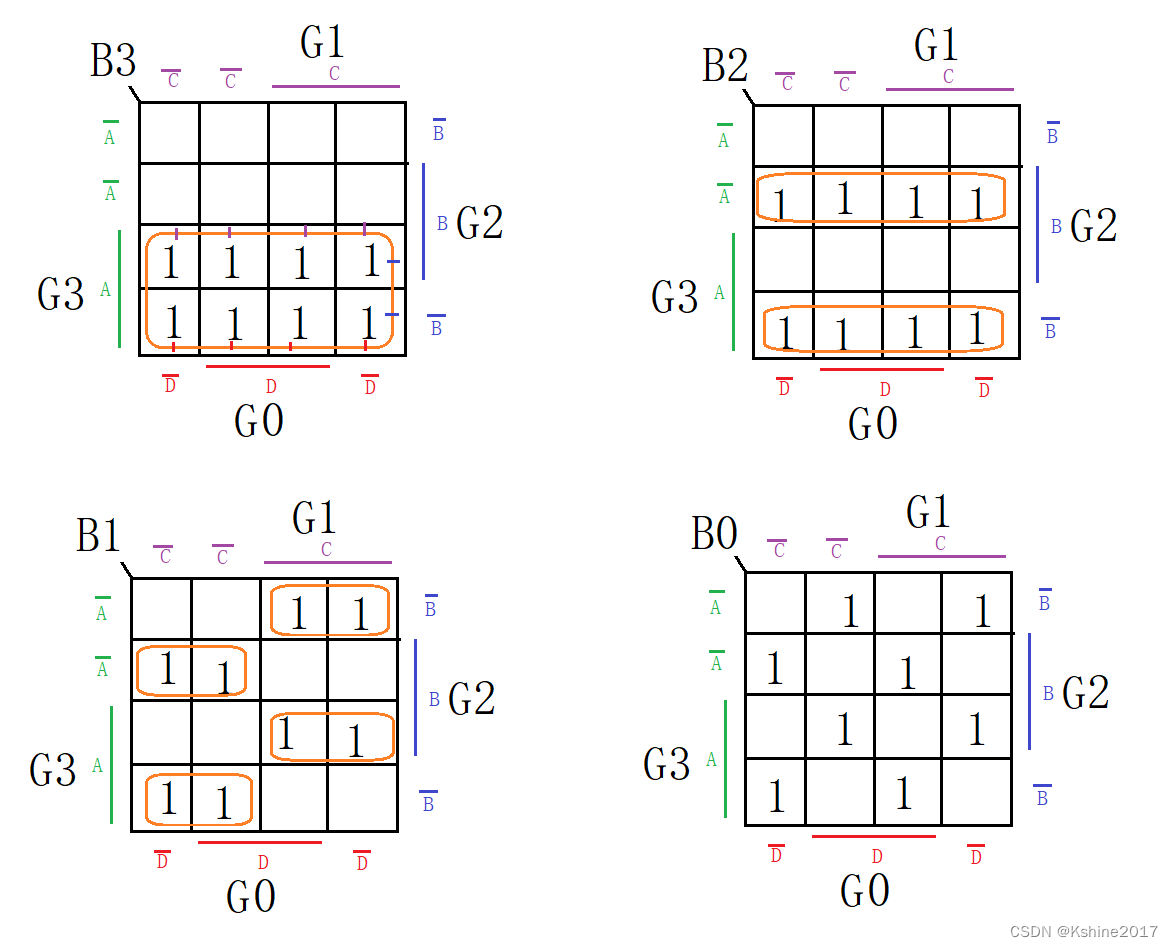
Lists logical expressions.
B
3
=
G
3
B_3 = G_3
B3=G3
B
2
=
G
3
‾
⋅
G
2
+
G
3
⋅
G
2
‾
=
G
3
⊕
G
2
B_2 = overline{G_3}·G_2 + G_3·overline{G_2}=G_3⊕G_2
B2=G3⋅G2+G3⋅G2=G3⊕G2
B
1
=
G
3
‾
G
2
G
1
‾
+
G
3
G
2
‾
G
1
‾
+
G
3
‾
G
2
‾
G
1
+
G
3
G
2
G
1
=
(
G
3
G
2
‾
+
G
3
‾
G
2
)
G
1
‾
+
(
G
3
G
2
‾
+
G
3
‾
G
2
)
‾
G
1
=
G
3
⊕
G
2
⊕
G
1
B_1 = overline{G_3}G_2overline{G_1}+G_3overline{G_2}overline{G_1}+overline{G_3}overline{G_2}G_1+G_3G_2G_1=(G_3overline{G_2}+overline{G_3}G_2)overline{G_1}+overline{(G_3overline{G_2}+overline{G_3}G_2)}G_1=G_3⊕G_2⊕G_1
B1=G3G2G1+G3G2G1+G3G2G1+G3G2G1=(G3G2+G3G2)G1+(G3G2+G3G2)G1=G3⊕G2⊕G1
B
0
=
G
3
⊕
G
2
⊕
G
1
⊕
G
0
B_0=G_3⊕G_2⊕G_1⊕G_0
B0=G3⊕G2⊕G1⊕G0
Draw a logic diagram.
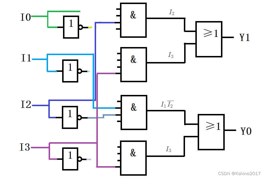
| I 0 I_0 I0 | I 1 I_1 I1 | I 2 I_2 I2 | I 3 I_3 I3 | Y 1 Y_1 Y1 | Y 0 Y_0 Y0 |
|---|---|---|---|---|---|
| 1 | 0 | 0 | 0 | 0 | 0 |
| 0 | 1 | 0 | 0 | 0 | 1 |
| 0 | 0 | 1 | 0 | 1 | 0 |
| 0 | 0 | 0 | 1 | 1 | 1 |
| I 0 I_0 I0 | I 1 I_1 I1 | I 2 I_2 I2 | I 3 I_3 I3 | Y 1 Y_1 Y1 | Y 0 Y_0 Y0 |
|---|---|---|---|---|---|
| 1 | 0 | 0 | 0 | 0 | 0 |
| X | 1 | 0 | 0 | 0 | 1 |
| X | X | 1 | 0 | 1 | 0 |
| X | X | X | 1 | 1 | 1 |
| S 9 S_9 S9 | S 8 S_8 S8 | S 7 S_7 S7 | S 6 S_6 S6 | S 5 S_5 S5 | S 4 S_4 S4 | S 3 S_3 S3 | S 2 S_2 S2 | S 1 S_1 S1 | S 0 S_0 S0 | A A A | B B B | C C C | D D D | G S GS GS | |
|---|---|---|---|---|---|---|---|---|---|---|---|---|---|---|---|
| 1 | 1 | 1 | 1 | 1 | 1 | 1 | 1 | 1 | 1 | 0 | 0 | 0 | 0 | 0 | |
| 1 | 1 | 1 | 1 | 1 | 1 | 1 | 1 | 1 | 0 | 0 | 0 | 0 | 0 | 1 | |
| 1 | 1 | 1 | 1 | 1 | 1 | 1 | 1 | 0 | 1 | 0 | 0 | 0 | 1 | 1 | |
| 1 | 1 | 1 | 1 | 1 | 1 | 1 | 0 | 1 | 1 | 0 | 0 | 1 | 0 | 1 | |
| 1 | 1 | 1 | 1 | 1 | 1 | 0 | 1 | 1 | 1 | 0 | 0 | 1 | 1 | 1 | |
| 1 | 1 | 1 | 1 | 1 | 0 | 1 | 1 | 1 | 1 | 0 | 1 | 0 | 0 | 1 | |
| 1 | 1 | 1 | 1 | 0 | 1 | 1 | 1 | 1 | 1 | 0 | 1 | 0 | 1 | 1 | |
| 1 | 1 | 1 | 0 | 1 | 1 | 1 | 1 | 1 | 1 | 0 | 1 | 1 | 0 | 1 | |
| 1 | 1 | 0 | 1 | 1 | 1 | 1 | 1 | 1 | 1 | 0 | 1 | 1 | 1 | 1 | |
| 1 | 0 | 1 | 1 | 1 | 1 | 1 | 1 | 1 | 1 | 1 | 0 | 0 | 0 | 1 | |
| 0 | 1 | 1 | 1 | 1 | 1 | 1 | 1 | 1 | 1 | 1 | 0 | 0 | 1 | 1 |
Typical: CD4532 priority encoder (discontinued)

Priority encoder I 7 has the highest priority, and I 0 has the lowest priority. Priority encoder I_7 has the highest priority, and I_0 has the lowest priority.Priority encoderI7The highest priority,I0Lowest priority.
When EI=1, all inputs are low level and noLower priorityInput high level, then output 000. At this time, EO=1.
EO = 1 only when EI = 1 and all inputs are 0. Dedicated to cascading with the EI of another device.
When EI=1, at least one of the input terminals is high level 1, GS=1.
For specific logical expressions and logic block diagrams, please refer to the book.
| EI Permitted Codes EI Permitted CodesEIAllow Encoding | I 7 I_7 I7 | I 6 I_6 I6 | I 5 I_5 I5 | I 4 I_4 I4 | I 3 I_3 I3 | I 2 I_2 I2 | I 1 I_1 I1 | I 0 I_0 I0 | Y 2 Y_2 Y2 | Y 1 Y_1 Y1 | Y 0 Y_0 Y0 | GS has input 1 GS has input 1GSWith input1 | EO input all 0 EO input all 0EOInput Full0 | |
|---|---|---|---|---|---|---|---|---|---|---|---|---|---|---|
| 0 | x | x | x | x | x | x | x | x | 0 | 0 | 0 | 0 | 0 | |
| 1 | 1 | x | x | x | x | x | x | x | 1 | 1 | 1 | 1 | 0 | |
| 1 | 0 | 1 | x | x | x | x | x | x | 1 | 1 | 0 | 1 | 0 | |
| 1 | 0 | 0 | 1 | x | x | x | x | x | 1 | 0 | 1 | 1 | 0 | |
| 1 | 0 | 0 | 0 | 1 | x | x | x | x | 1 | 0 | 0 | 1 | 0 | |
| 1 | 0 | 0 | 0 | 0 | 1 | x | x | x | 0 | 1 | 1 | 1 | 0 | |
| 1 | 0 | 0 | 0 | 0 | 0 | 1 | x | x | 0 | 1 | 0 | 1 | 0 | |
| 1 | 0 | 0 | 0 | 0 | 0 | 0 | 1 | x | 0 | 0 | 1 | 1 | 0 | |
| 1 | 0 | 0 | 0 | 0 | 0 | 0 | 0 | 1 | 0 | 0 | 0 | 1 | 0 | |
| 1 | 0 | 0 | 0 | 0 | 0 | 0 | 0 | 0 | 0 | 0 | 0 | 0 | 1 |

When EI 1 = 0, slice 1 is disabled. Y 2 Y 1 Y 0 = = 000, GS 1 = 0, EO 1 = 0. EI 0 = 0, slice 0 is also disabled. When EI_1=0, slice 1 is disabled. Y_2Y_1Y_0==000, GS_1=0, EO_1=0. EI_0=0, slice 0 is also disabled.whenEI1=0Time, piece1Disabled.Y2Y1Y0==000,GS1=0,EO1=0。EI0=0,piece0is also disabled.
When EI 1 = 1, encoding is allowed for slice 1. If I 15 − I 8 = 000...000, then EO 1 = 1, and thus EI 0 = 1. Encoding is allowed for slice 0. It can be seen that the priority of encoding for slice 1 is higher than that of encoding for slice 0. When EI_1=1, encoding is allowed for slice 1. If I_{15} - I_8 = 000...000, then EO_1=1, and thus EI_0=1. Encoding is allowed for slice 0. It can be seen that the priority of encoding for slice 1 is higher than that of encoding for slice 0.whenEI1=1Time, piece1Encoding is allowed ifI15−I8=000...000,at this timeEO1=1,therebyEI0=1.piece0Encoding is allowed.1Encoding takes precedence over slices0coding。
When EI 1 = 1, encoding is allowed for slice 1. If I 15 − I 8 has at least one 1, then EO 1 = 0, thus EI 0 = 0, and encoding is prohibited for slice 0. When EI_1=1, encoding is allowed for slice 1. If I_{15} - I_8 has at least one 1, then EO_1=0, thus EI_0=0, and encoding is prohibited for slice 0.whenEI1=1Time, piece1Encoding is allowed ifI15−I8at least one1,at this timeEO1=0,therebyEI0=0,piece0Encoding is prohibited.
| EI 1 Allowed Encoding EI_1 Allowed EncodingEI1Allow Encoding | EI 0 Allowed encoding EI_0 Allowed encodingEI0Allow Encoding | I 15 I_{15} I15 | I 14 I_{14} I14 | I 13 I_{13} I13 | I 12 I_{12} I12 | I 11 I_{11} I11 | I 10 I_{10} I10 | I 9 I_{9} I9 | I 8 I_8 I8 | I 7 I_7 I7 | I 6 I_6 I6 | I 5 I_5 I5 | I 4 I_4 I4 | I 3 I_3 I3 | I 2 I_2 I2 | I 1 I_1 I1 | I 0 I_0 I0 | Y 2 1 Y2_1 Y21 | Y 1 1 Y1_1 Y11 | Y 0 1 Y0_1 Y01 | Y 2 0 Y2_0 Y20 | Y 1 0 Y1_0 Y10 | Y 0 0 Y0_0 Y00 | EO 1 input all 0 EO_1 input all 0EO1Input Full0 | EO 0 Input all 0 EO_0 Input all 0EO0Input Full0 | GS 1 has input 1 GS_1 has input 1GS1With input1 | GS 0 has input 0 GS_0 has input 0GS0With input0 | L 3 L_3 L3 | L 2 L_2 L2 | L 1 L_1 L1 | L 0 L_0 L0 | |
|---|---|---|---|---|---|---|---|---|---|---|---|---|---|---|---|---|---|---|---|---|---|---|---|---|---|---|---|---|---|---|---|---|
| 0 (slice 1 disabled) | E I 0 = E O 1 = 0 EI_0=EO_1=0 EI0=EO1=0(Disabled for slice 0) | x | x | x | x | x | x | x | x | x | x | x | x | x | x | x | x | 0 | 0 | 0 | 0 | 0 | 0 | 0 | 0 | 0 | 0 | 0 | 0 | 0 | 0 | |
| 1 | 0 | 1 | x | x | x | x | x | x | x | x | x | x | x | x | x | x | x | 1 | 1 | 1 | 0 | 0 | 0 | 0 | 0 | 1 (Chip 1 has input) | 0 | 1 L 3 = G S 1 L_3 =GS_1 L3=GS1 | 1 L 2 = Y 2 1 L_2 =Y2_1 L2=Y21 | 1 L 1 = Y 1 1 L_1 =Y1_1 L1=Y11 | 1 L 0 = Y 0 1 L_0 =Y0_1 L0=Y01 | |
| 1 | 0 | 0 | 1 | x | x | x | x | x | x | x | x | x | x | x | x | x | x | 1 | 1 | 0 | 0 | 0 | 0 | 0 | 0 | 1 | 0 | 1 | 1 | 1 | 0 | |
| 1 | 0 | 0 | 0 | 1 | x | x | x | x | x | x | x | x | x | x | x | x | x | 1 | 0 | 1 | 0 | 0 | 0 | 0 | 0 | 1 | 0 | 1 | 1 | 0 | 1 | |
| 1 | 0 | 0 | 0 | 0 | 1 | x | x | x | x | x | x | x | x | x | x | x | x | 1 | 0 | 0 | 0 | 0 | 0 | 0 | 0 | 1 | 0 | 1 | 1 | 0 | 0 | |
| 1 | 0 | 0 | 0 | 0 | 0 | 1 | x | x | x | x | x | x | x | x | x | x | x | 0 | 1 | 1 | 0 | 0 | 0 | 0 | 0 | 1 | 0 | 1 | 0 | 1 | 1 | |
| 1 | 0 | 0 | 0 | 0 | 0 | 0 | 1 | x | x | x | x | x | x | x | x | x | x | 0 | 1 | 0 | 0 | 0 | 0 | 0 | 0 | 1 | 0 | 1 | 0 | 1 | 0 | |
| 1 | 0 | 0 | 0 | 0 | 0 | 0 | 0 | 1 | x | x | x | x | x | x | x | x | x | 0 | 0 | 1 | 0 | 0 | 0 | 0 | 0 | 1 | 0 | 1 | 0 | 0 | 1 | |
| 1 | 0 | 0 | 0 | 0 | 0 | 0 | 0 | 0 | 1 | x | x | x | x | x | x | x | x | 0 | 0 | 0 | 0 | 0 | 0 | 0 | 0 | 1 | 0 | 1 | 0 | 0 | 0 | |
| 1 | E I 0 = E O 1 = 1 EI_0=EO_1=1 EI0=EO1=1(Slice 0 working) | 0 | 0 | 0 | 0 | 0 | 0 | 0 | 0 | 1 | x | x | x | x | x | x | x | 0 | 0 | 0 | 1 | 1 | 1 | 1 (chip 1 input all 0) | 0 | 0 (chip 1 invalid code) | 1 | 0 L 3 = G S 1 L_3 =GS_1 L3=GS1 | 1 L 2 = Y 2 0 L_2 =Y2_0 L2=Y20 | 1 L 1 = Y 1 0 L_1 =Y1_0 L1=Y10 | 1 L 0 = Y 0 0 L_0 =Y0_0 L0=Y00 | |
| 1 | 1 | 0 | 0 | 0 | 0 | 0 | 0 | 0 | 0 | 0 | 1 | x | x | x | x | x | x | 0 | 0 | 0 | 1 | 1 | 0 | 1 | 0 | 0 | 1 | 0 | 1 | 1 | 0 | |
| 1 | 1 | 0 | 0 | 0 | 0 | 0 | 0 | 0 | 0 | 0 | 0 | 1 | x | x | x | x | x | 0 | 0 | 0 | 1 | 1 | 1 | 1 | 0 | 0 | 1 | 0 | 1 | 0 | 1 | |
| 1 | 1 | 0 | 0 | 0 | 0 | 0 | 0 | 0 | 0 | 0 | 0 | 0 | 1 | x | x | x | x | 0 | 0 | 0 | 1 | 1 | 1 | 1 | 0 | 0 | 1 | 0 | 1 | 0 | 0 | |
| 1 | 1 | 0 | 0 | 0 | 0 | 0 | 0 | 0 | 0 | 0 | 0 | 0 | 0 | 1 | x | x | x | 0 | 0 | 0 | 1 | 1 | 1 | 1 | 0 | 0 | 1 | 0 | 0 | 1 | 1 | |
| 1 | 1 | 0 | 0 | 0 | 0 | 0 | 0 | 0 | 0 | 0 | 0 | 0 | 0 | 0 | 1 | x | x | 0 | 0 | 0 | 1 | 1 | 1 | 1 | 0 | 0 | 1 | 0 | 0 | 1 | 0 | |
| 1 | 1 | 0 | 0 | 0 | 0 | 0 | 0 | 0 | 0 | 0 | 0 | 0 | 0 | 0 | 0 | 1 | x | 0 | 0 | 0 | 1 | 1 | 1 | 1 | 0 | 0 | 1 | 0 | 0 | 0 | 1 | |
| 1 | 1 | 0 | 0 | 0 | 0 | 0 | 0 | 0 | 0 | 0 | 0 | 0 | 0 | 0 | 0 | 0 | 1 | 0 | 0 | 0 | 1 | 1 | 1 | 1 | 0 | 0 | 1 | 0 | 0 | 0 | 0 | |
| 1 | 1 | 0 | 0 | 0 | 0 | 0 | 0 | 0 | 0 | 0 | 0 | 0 | 0 | 0 | 0 | 0 | 0 | 0 | 0 | 0 | 1 | 1 | 1 | 1 | 1 (chip 0 input all 0) | 0 | 0 (chip 0 invalid code) | 0 | 0 | 0 | 0 |

| enter | Output | |||||
| /E | A_1 | A_0 | /Y_3 | /Y_2 | /Y_1 | /Y_0 |
| 1. Prohibition | X | X | 1 | 1 | 1 | 1 |
| 0 Enable | 0 | 0 | 1 | 1 | 1 | 0 Low effective |
| 0 Enable | 0 | 1 | 1 | 1 | 0 low effective | 1 |
| 0 Enable | 1 | 0 | 1 | 0 Low effective | 1 | 1 |
| 0 Enable | 1 | 1 | 0 Low effective | 1 | 1 | 1 |
Y
0
‾
=
E
‾
‾
⋅
A
1
‾
⋅
A
0
‾
‾
overline{Y_0} = overline{overline{overline{E}}·overline{A_1}·overline{A_0}}
Y0=E⋅A1⋅A0 //00
Y
1
‾
=
E
‾
‾
⋅
A
1
‾
⋅
A
0
‾
overline{Y_1} = overline{overline{overline{E}}·overline{A_1}·A_0}
Y1=E⋅A1⋅A0 //01
Y
2
‾
=
E
‾
‾
⋅
A
1
⋅
A
0
‾
‾
overline{Y_2} = overline{overline{overline{E}}·A_1·overline{A_0}}
Y2=E⋅A1⋅A0 //10
Y
3
‾
=
E
‾
‾
⋅
A
1
⋅
A
0
‾
overline{Y_3} = overline{overline{overline{E}}·A_1·A_0}
Y3=E⋅A1⋅A0 //11


Y
0
‾
=
E
3
⋅
E
2
‾
‾
⋅
E
1
‾
‾
⋅
A
2
‾
⋅
A
1
‾
⋅
A
0
‾
‾
overline{Y_0} = overline{E_3·overline{overline{E_2}}·overline{overline{E_1}}·overline{A_2}·overline{A_1}·overline{A_0}}
Y0=E3⋅E2⋅E1⋅A2⋅A1⋅A0 //000
Y
1
‾
=
E
3
⋅
E
2
‾
‾
⋅
E
1
‾
‾
⋅
A
2
‾
⋅
A
1
‾
⋅
A
0
‾
overline{Y_1} = overline{E_3·overline{overline{E_2}}·overline{overline{E_1}}·overline{A_2}·overline{A_1}·A_0}
Y1=E3⋅E2⋅E1⋅A2⋅A1⋅A0 //001
Y
2
‾
=
E
3
⋅
E
2
‾
‾
⋅
E
1
‾
‾
⋅
A
2
‾
⋅
A
1
⋅
A
0
‾
‾
overline{Y_2} = overline{E_3·overline{overline{E_2}}·overline{overline{E_1}}·overline{A_2}·A_1·overline{A_0}}
Y2=E3⋅E2⋅E1⋅A2⋅A1⋅A0 //010
Y
3
‾
=
E
3
⋅
E
2
‾
‾
⋅
E
1
‾
‾
⋅
A
2
‾
⋅
A
1
⋅
A
0
‾
overline{Y_3} = overline{E_3·overline{overline{E_2}}·overline{overline{E_1}}·overline{A_2}·A_1·A_0}
Y3=E3⋅E2⋅E1⋅A2⋅A1⋅A0 //011
Y
4
‾
=
E
3
⋅
E
2
‾
‾
⋅
E
1
‾
‾
⋅
A
2
⋅
A
1
‾
⋅
A
0
‾
‾
overline{Y_4} = overline{E_3·overline{overline{E_2}}·overline{overline{E_1}}·A_2·overline{A_1}·overline{A_0}}
Y4=E3⋅E2⋅E1⋅A2⋅A1⋅A0 //100
Y
5
‾
=
E
3
⋅
E
2
‾
‾
⋅
E
1
‾
‾
⋅
A
2
⋅
A
1
‾
⋅
A
0
‾
overline{Y_5} = overline{E_3·overline{overline{E_2}}·overline{overline{E_1}}·A_2·overline{A_1}·A_0}
Y5=E3⋅E2⋅E1⋅A2⋅A1⋅A0 //101
Y
6
‾
=
E
3
⋅
E
2
‾
‾
⋅
E
1
‾
‾
⋅
A
2
⋅
A
1
⋅
A
0
‾
‾
overline{Y_6} = overline{E_3·overline{overline{E_2}}·overline{overline{E_1}}·A_2·A_1·overline{A_0}}
Y6=E3⋅E2⋅E1⋅A2⋅A1⋅A0 //110
Y
7
‾
=
E
3
⋅
E
2
‾
‾
⋅
E
1
‾
‾
⋅
A
2
⋅
A
1
⋅
A
0
‾
overline{Y_7} = overline{E_3·overline{overline{E_2}}·overline{overline{E_1}}·A_2·A_1·A_0}
Y7=E3⋅E2⋅E1⋅A2⋅A1⋅A0 //111

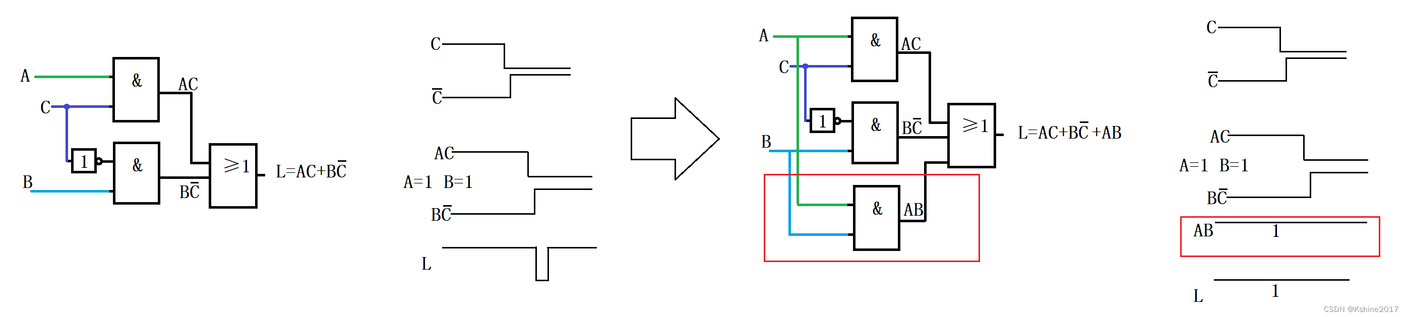
L = A ‾ ⋅ C ‾ + A ⋅ B = A ‾ ⋅ B ‾ ⋅ C ‾ + A ‾ ⋅ B ⋅ C ‾ + A ⋅ B ⋅ C ‾ + A B C = m 0 + m 2 + m 6 + m 7 L=overline{A}·overline{C}+A·B =overline{A}·overline{B}·overline{C}+overline{A}·B·overline{C} + A·B·overline{C}+ABC = m_0+m_2+m_6+m_7 L=A⋅C+A⋅B=A⋅B⋅C+A⋅B⋅C+A⋅B⋅C+ABC=m0+m2+m6+m7
Y
0
‾
=
E
3
⋅
E
2
‾
‾
⋅
E
1
‾
‾
⋅
A
2
‾
⋅
A
1
‾
⋅
A
0
‾
‾
=
E
3
⋅
E
2
‾
‾
⋅
E
1
‾
‾
⋅
m
0
‾
overline{Y_0} = overline{E_3·overline{overline{E_2}}·overline{overline{E_1}}·overline{A_2}·overline{A_1}·overline{A_0}} = overline{E_3·overline{overline{E_2}}·overline{overline{E_1}}·m_0}
Y0=E3⋅E2⋅E1⋅A2⋅A1⋅A0=E3⋅E2⋅E1⋅m0 //000
Y
1
‾
=
E
3
⋅
E
2
‾
‾
⋅
E
1
‾
‾
⋅
A
2
‾
⋅
A
1
‾
⋅
A
0
‾
=
E
3
⋅
E
2
‾
‾
⋅
E
1
‾
‾
⋅
m
1
‾
overline{Y_1} = overline{E_3·overline{overline{E_2}}·overline{overline{E_1}}·overline{A_2}·overline{A_1}·A_0} = overline{E_3·overline{overline{E_2}}·overline{overline{E_1}}·m_1}
Y1=E3⋅E2⋅E1⋅A2⋅A1⋅A0=E3⋅E2⋅E1⋅m1 //001
Y
2
‾
=
E
3
⋅
E
2
‾
‾
⋅
E
1
‾
‾
⋅
A
2
‾
⋅
A
1
⋅
A
0
‾
‾
=
E
3
⋅
E
2
‾
‾
⋅
E
1
‾
‾
⋅
m
2
‾
overline{Y_2} = overline{E_3·overline{overline{E_2}}·overline{overline{E_1}}·overline{A_2}·A_1·overline{A_0}}= overline{E_3·overline{overline{E_2}}·overline{overline{E_1}}·m_2}
Y2=E3⋅E2⋅E1⋅A2⋅A1⋅A0=E3⋅E2⋅E1⋅m2 //010
Y
3
‾
=
E
3
⋅
E
2
‾
‾
⋅
E
1
‾
‾
⋅
A
2
‾
⋅
A
1
⋅
A
0
‾
=
E
3
⋅
E
2
‾
‾
⋅
E
1
‾
‾
⋅
m
3
‾
overline{Y_3} = overline{E_3·overline{overline{E_2}}·overline{overline{E_1}}·overline{A_2}·A_1·A_0}= overline{E_3·overline{overline{E_2}}·overline{overline{E_1}}·m_3}
Y3=E3⋅E2⋅E1⋅A2⋅A1⋅A0=E3⋅E2⋅E1⋅m3 //011
Y
4
‾
=
E
3
⋅
E
2
‾
‾
⋅
E
1
‾
‾
⋅
A
2
⋅
A
1
‾
⋅
A
0
‾
‾
=
E
3
⋅
E
2
‾
‾
⋅
E
1
‾
‾
⋅
m
4
‾
overline{Y_4} = overline{E_3·overline{overline{E_2}}·overline{overline{E_1}}·A_2·overline{A_1}·overline{A_0}}= overline{E_3·overline{overline{E_2}}·overline{overline{E_1}}·m_4}
Y4=E3⋅E2⋅E1⋅A2⋅A1⋅A0=E3⋅E2⋅E1⋅m4 //100
Y
5
‾
=
E
3
⋅
E
2
‾
‾
⋅
E
1
‾
‾
⋅
A
2
⋅
A
1
‾
⋅
A
0
‾
=
E
3
⋅
E
2
‾
‾
⋅
E
1
‾
‾
⋅
m
5
‾
overline{Y_5} = overline{E_3·overline{overline{E_2}}·overline{overline{E_1}}·A_2·overline{A_1}·A_0}= overline{E_3·overline{overline{E_2}}·overline{overline{E_1}}·m_5}
Y5=E3⋅E2⋅E1⋅A2⋅A1⋅A0=E3⋅E2⋅E1⋅m5 //101
Y
6
‾
=
E
3
⋅
E
2
‾
‾
⋅
E
1
‾
‾
⋅
A
2
⋅
A
1
⋅
A
0
‾
‾
=
E
3
⋅
E
2
‾
‾
⋅
E
1
‾
‾
⋅
m
6
‾
overline{Y_6} = overline{E_3·overline{overline{E_2}}·overline{overline{E_1}}·A_2·A_1·overline{A_0}}= overline{E_3·overline{overline{E_2}}·overline{overline{E_1}}·m_6}
Y6=E3⋅E2⋅E1⋅A2⋅A1⋅A0=E3⋅E2⋅E1⋅m6 //110
Y
7
‾
=
E
3
⋅
E
2
‾
‾
⋅
E
1
‾
‾
⋅
A
2
⋅
A
1
⋅
A
0
‾
=
E
3
⋅
E
2
‾
‾
⋅
E
1
‾
‾
⋅
m
7
‾
overline{Y_7} = overline{E_3·overline{overline{E_2}}·overline{overline{E_1}}·A_2·A_1·A_0}= overline{E_3·overline{overline{E_2}}·overline{overline{E_1}}·m_7}
Y7=E3⋅E2⋅E1⋅A2⋅A1⋅A0=E3⋅E2⋅E1⋅m7 //111
Ensure E 3 = 1 , E 2 = 0 , E 1 = 0 Ensure E_3=1,E_2=0,E_1=0make sureE3=1,E2=0,E1=0, that is to say Y 0 ‾ = m 0 ‾ , Y 2 ‾ = m 2 ‾ , Y 6 ‾ = m 6 ‾ , Y 7 ‾ = m 7 ‾ overline{Y_0}=overline{m_0},overline{Y_2}=overline{m_2},overline{Y_6}=overline{m_6},overline{Y_7}=overline{m_7} Y0=m0,Y2=m2,Y6=m6,Y7=m7。
Transformation of the logistic function according to the inversion law
L
=
L
‾
‾
=
m
0
+
m
2
+
m
6
+
m
7
‾
‾
=
m
0
‾
⋅
m
2
‾
⋅
m
6
‾
⋅
m
7
‾
‾
=
m
0
+
m
2
+
m
6
+
m
7
‾
‾
=
Y
0
‾
⋅
Y
2
‾
⋅
Y
6
‾
⋅
Y
7
‾
‾
L=overline{overline{L}} = overline{overline{m_0+m_2+m_6+m_7}} = overline{overline{m_0}·overline{m_2}·overline{m_6}·overline{m_7}} = overline{overline{m_0+m_2+m_6+m_7}} = overline{overline{Y_0}·overline{Y_2}·overline{Y_6}·overline{Y_7}}
L=L=m0+m2+m6+m7=m0⋅m2⋅m6⋅m7=m0+m2+m6+m7=Y0⋅Y2⋅Y6⋅Y7
Get the logic diagram

774HC42
4 input ports
10 output terminals, output low level is valid, corresponding to decimal numbers 0~9.

4 input terminals, 16 conditions in total
only m 0 , m 1 , m 2 . . . . . . m 9 m_0 ,m_1,m_2......m_9 m0,m1,m2......m9It is a valid input (the corresponding output pin outputs low 0, and the rest output high 1).
The remaining 6 m 10 , m 11 , m 12 . . . . . . m 15 m_{10} ,m_{11},m_{12}......m_{15} m10,m11,m12......m15There is no valid decoding output (when invalid, all outputs are high 1).
Draw the input and output waveforms of 74HC42.


Digital tube display principle

Integrated seven-segment display decoder. 74HC4511 (common cathode) (high level lights up)
L E LE LELatch Enable
L T ‾ overline{LT} LTLamp test input, when L T ‾ = 0 overline{LT}=0 LT=0When , ag outputs all 1s and displays the character "8".
B
L
‾
overline{BL}
BLLight off input, when LT ‾ = 1, and BL ‾ = 1 overline{LT}=1, and overline{BL}=1LT=1,andBL=1When , ag outputs all 0. It can be used to turn off unnecessary displayed zero "0".

D 3 D 2 D 1 D 0 D_3D_2D_1D_0 D3D2D1D0=0000, the corresponding output character is "0"
D 3 D 2 D 1 D 0 D_3D_2D_1D_0 D3D2D1D0=0001, the corresponding output character is "1"
D 3 D 2 D 1 D 0 D_3D_2D_1D_0 D3D2D1D0=0010, the corresponding output font is "2"
D 3 D 2 D 1 D 0 D_3D_2D_1D_0 D3D2D1D0=0011, the corresponding output character is "3"
D 3 D 2 D 1 D 0 D_3D_2D_1D_0 D3D2D1D0=0100, the corresponding output font is "4"
D 3 D 2 D 1 D 0 D_3D_2D_1D_0 D3D2D1D0=0101, the corresponding output character is "5"
D 3 D 2 D 1 D 0 D_3D_2D_1D_0 D3D2D1D0=0110, the corresponding output character is "6"
D 3 D 2 D 1 D 0 D_3D_2D_1D_0 D3D2D1D0=0111, the corresponding output character is "7"
D 3 D 2 D 1 D 0 D_3D_2D_1D_0 D3D2D1D0=1000, the corresponding output font is "8"
D 3 D 2 D 1 D 0 D_3D_2D_1D_0 D3D2D1D0=1001, the corresponding output font is "9"
1010-1111, off
One to many, send the data of the public data line to different channels as needed.
Similar to "SPMT switch"
Using unique address decoder to implement data distributor
For example, 74x138 integrates a 3-line to 8-line decoder.
E 1 – as data input overline{E_1} as data inputE1As data input
Y
0
Y
1
Y
2
Y
3
Y
4
Y
5
Y
6
Y
7
Y_0 Y_1 Y_2Y_3Y_4Y_5Y_6Y_7
Y0Y1Y2Y3Y4Y5Y6Y78 channels as data output

Y 2 ‾ = E 3 ⋅ E 2 ‾ ‾ ⋅ E 1 ‾ ‾ ⋅ A 2 ‾ ⋅ A 1 ⋅ A 0 ‾ ‾ overline{Y_2} = overline{E_3·overline{overline{E_2}}·overline{overline{E_1}}·overline{A_2}·A_1·overline{A_0}} Y2=E3⋅E2⋅E1⋅A2⋅A1⋅A0 //010
Above, E 3 = 1 , E 2 ‾ = 0 E_3=1,overline{E_2}=0 E3=1,E2=0, when the address line A 2 A 1 A 0 = 010 A_2A_1A_0=010 A2A1A0=010hour, Y 2 ‾ = E 1 ‾ overline{Y_2}=overline{E_1} Y2=E1
Similarly, we can conclude that:
When the address line
A
2
A
1
A
0
=
000
A_2A_1A_0=000
A2A1A0=000hour,
Y
0
‾
=
E
1
‾
=
D
overline{Y_0}=overline{E_1}=D
Y0=E1=D,other
Y
x
=
1
Y_x=1
Yx=1。
When the address line
A
2
A
1
A
0
=
001
A_2A_1A_0=001
A2A1A0=001hour,
Y
1
‾
=
E
1
‾
=
D
overline{Y_1}=overline{E_1}=D
Y1=E1=D,other
Y
x
=
1
Y_x=1
Yx=1。
When the address line
A
2
A
1
A
0
=
010
A_2A_1A_0=010
A2A1A0=010hour,
Y
2
‾
=
E
1
‾
=
D
overline{Y_2}=overline{E_1}=D
Y2=E1=D,other
Y
x
=
1
Y_x=1
Yx=1。
When the address line
A
2
A
1
A
0
=
011
A_2A_1A_0=011
A2A1A0=011hour,
Y
3
‾
=
E
1
‾
=
D
overline{Y_3}=overline{E_1}=D
Y3=E1=D,other
Y
x
=
1
Y_x=1
Yx=1。
When the address line
A
2
A
1
A
0
=
100
A_2A_1A_0=100
A2A1A0=100hour,
Y
4
‾
=
E
1
‾
=
D
overline{Y_4}=overline{E_1}=D
Y4=E1=D,other
Y
x
=
1
Y_x=1
Yx=1。
When the address line
A
2
A
1
A
0
=
101
A_2A_1A_0=101
A2A1A0=101hour,
Y
5
‾
=
E
1
‾
=
D
overline{Y_5}=overline{E_1}=D
Y5=E1=D,other
Y
x
=
1
Y_x=1
Yx=1。
When the address line
A
2
A
1
A
0
=
110
A_2A_1A_0=110
A2A1A0=110hour,
Y
6
‾
=
E
1
‾
=
D
overline{Y_6}=overline{E_1}=D
Y6=E1=D,other
Y
x
=
1
Y_x=1
Yx=1。
When the address line
A
2
A
1
A
0
=
111
A_2A_1A_0=111
A2A1A0=111hour,
Y
7
‾
=
E
1
‾
=
D
overline{Y_7}=overline{E_1}=D
Y7=E1=D,other
Y
x
=
1
Y_x=1
Yx=1。

Y
=
S
2
‾
⋅
S
1
‾
⋅
S
0
‾
⋅
D
0
+
S
2
‾
⋅
S
1
‾
⋅
S
0
⋅
D
1
+
S
2
‾
⋅
S
1
⋅
S
0
‾
⋅
D
2
+
S
2
‾
⋅
S
1
⋅
S
0
⋅
D
3
+
S
2
⋅
S
1
‾
⋅
S
0
‾
⋅
D
4
+
S
2
⋅
S
1
‾
⋅
S
0
⋅
D
5
+
S
2
⋅
S
1
⋅
S
0
‾
⋅
D
6
+
S
2
⋅
S
1
⋅
S
0
⋅
D
7
Y=overline{S_2}·overline{S_1}·overline{S_0}·D_0 +overline{S_2}·overline{S_1}·S_0·D_1 +overline{S_2}·S_1·overline{S_0}·D_2 +overline{S_2}·S_1·S_0·D_3 +S_2·overline{S_1}·overline{S_0}·D_4 +S_2·overline{S_1}·S_0·D_5 +S_2·S_1·overline{S_0}·D_6 +S_2·S_1·S_0·D_7
Y=S2⋅S1⋅S0⋅D0+S2⋅S1⋅S0⋅D1+S2⋅S1⋅S0⋅D2+S2⋅S1⋅S0⋅D3+S2⋅S1⋅S0⋅D4+S2⋅S1⋅S0⋅D5+S2⋅S1⋅S0⋅D6+S2⋅S1⋅S0⋅D7

Extensions to data selectors.
Logical Function Generator
Known, 8 to 1 data selector.
Y
=
S
2
‾
⋅
S
1
‾
⋅
S
0
‾
⋅
D
0
+
S
2
‾
⋅
S
1
‾
⋅
S
0
⋅
D
1
+
S
2
‾
⋅
S
1
⋅
S
0
‾
⋅
D
2
+
S
2
‾
⋅
S
1
⋅
S
0
⋅
D
3
+
S
2
⋅
S
1
‾
⋅
S
0
‾
⋅
D
4
+
S
2
⋅
S
1
‾
⋅
S
0
⋅
D
5
+
S
2
⋅
S
1
⋅
S
0
‾
⋅
D
6
+
S
2
⋅
S
1
⋅
S
0
⋅
D
7
Y=overline{S_2}·overline{S_1}·overline{S_0}·D_0 +overline{S_2}·overline{S_1}·S_0·D_1 +overline{S_2}·S_1·overline{S_0}·D_2 +overline{S_2}·S_1·S_0·D_3 +S_2·overline{S_1}·overline{S_0}·D_4 +S_2·overline{S_1}·S_0·D_5 +S_2·S_1·overline{S_0}·D_6 +S_2·S_1·S_0·D_7
Y=S2⋅S1⋅S0⋅D0+S2⋅S1⋅S0⋅D1+S2⋅S1⋅S0⋅D2+S2⋅S1⋅S0⋅D3+S2⋅S1⋅S0⋅D4+S2⋅S1⋅S0⋅D5+S2⋅S1⋅S0⋅D6+S2⋅S1⋅S0⋅D7
Y = m 0 ⋅ D 0 + m 1 ⋅ D 1 + m 2 ⋅ D 2 + m 3 ⋅ D 3 + m 4 ⋅ D 4 + m 5 ⋅ D 5 + m 6 ⋅ D 6 + m 7 ⋅ D 7 Y=m_0·D_0 +m_1·D_1 +m_2·D_2 +m_3·D_3 +m_4·D_4 +m_5·D_5 +m_6·D_6 +m_7·D_7 Y=m0⋅D0+m1⋅D1+m2⋅D2+m3⋅D3+m4⋅D4+m5⋅D5+m6⋅D6+m7⋅D7
Logical functions
L
=
A
‾
B
C
+
A
B
‾
C
+
A
B
L=overline{A}BC+Aoverline{B}C+AB
L=ABC+ABC+AB
L
=
A
‾
B
C
+
A
B
‾
C
+
A
B
=
A
‾
B
C
+
A
B
‾
C
+
A
B
C
‾
+
A
B
C
=
m
3
+
m
5
+
m
6
+
m
7
L=overline{A}BC+Aoverline{B}C+AB=overline{A}BC+Aoverline{B}C+ABoverline{C}+ABC=m_3+m_5+m_6+m_7
L=ABC+ABC+AB=ABC+ABC+ABC+ABC=m3+m5+m6+m7
Use 8 to 1 data selector to implement the above function L
L = Y = m 3 + m 5 + m 6 + m 7 , where D 7 D 6 D 5 D 3 = 1111 , D 4 D 2 D 1 D 0 = 0000 L = Y = m_3+m_5+m_6+m_7 , where D_7D_6D_5D_3=1111 , D_4D_2D_1D_0=0000L=Y=m3+m5+m6+m7,inD7D6D5D3=1111,D4D2D1D0=0000

Parallel data to serial data

| A | B | F A > B F_{A>B} FA>B | F A < B F_{A<B} FA<B | F A = = B F_{A==B} FA==B |
|---|---|---|---|---|
| 0 | 0 | 0 | 0 | 1 |
| 0 | 1 | 0 | 1 | 0 |
| 1 | 0 | 1 | 0 | 0 |
| 1 | 1 | 0 | 0 | 1 |

| A 1 ? B 1 A _1?B_1 A1?B1 | A 0 ? B 0 A_0?B_0 A0?B0 | F A > B F_{A>B} FA>B | F A < B F_{A<B} FA<B | F A = = B F_{A==B} FA==B |
|---|---|---|---|---|
| A 1 > B 1 A_1>B_1 A1>B1 | x | 1 | 0 | 0 |
| A 1 < B 1 A_1<B_1 A1<B1 | x | 0 | 1 | 0 |
| A 1 = = B 1 A_1==B_1 A1==B1 | A 0 > B 0 A_0>B_0 A0>B0 | 1 | 0 | 0 |
| A 1 = = B 1 A_1==B_1 A1==B1 | A 0 < B 0 A_0<B_0 A0<B0 | 0 | 1 | 0 |
| A 1 = = B 1 A_1==B_1 A1==B1 | A 0 = = B 0 A_0==B_0 A0==B0 | 0 | 0 | 1 |
Logical expressions
F
A
>
B
=
F
A
1
>
B
1
+
F
A
1
=
=
B
1
⋅
F
A
0
>
B
0
F_{A>B} = F_{A_1>B_1} +F_{A_1==B_1}·F_{A_0>B_0}
FA>B=FA1>B1+FA1==B1⋅FA0>B0
F
A
<
B
=
F
A
1
<
B
1
+
F
A
1
=
=
B
1
⋅
F
A
0
<
B
0
F_{A<B} = F_{A_1<B_1} +F_{A_1==B_1}·F_{A_0<B_0}
FA<B=FA1<B1+FA1==B1⋅FA0<B0
F
A
=
=
B
=
F
A
1
=
=
B
1
⋅
F
A
0
=
=
B
0
F_{A==B} = F_{A_1==B_1}·F_{A_0==B_0}
FA==B=FA1==B1⋅FA0==B0
Logic diagram


Connect in series to expand to 8-bit value comparator

Connect in parallel and expand to a 16-bit numerical comparator.
When connected in parallel, the speed is fast.


I have devoted myself to the research of technology for more than 30 years. I am proficient in various languages such as Java, Linux, JavaScript, PHP, CSS, etc. I have made many contributions in the field of open source. I have established a developer documentation site to share some problems in technology development for everyone to read.