2024-07-12
한어Русский языкEnglishFrançaisIndonesianSanskrit日本語DeutschPortuguêsΕλληνικάespañolItalianoSuomalainenLatina
At present, there are two solutions for FPGA to realize SDI video codec: one is to use dedicated codec chips, such as the typical receiver GS2971 and transmitter GS2972. The advantage is simplicity. For example, the GS2971 receiver directly decodes SDI into parallel YCrCb422, and the GS2972 transmitter directly encodes parallel YCrCb422 into SDI video. The disadvantage is high cost. You can search the prices of GS2971 and GS2972 on Baidu. The other solution is to use FPGA logic resources to realize SDI codec, use the GTP/GTX resources of Xilinx series FPGA to realize deserialization, and use the SMPTE SDI resources of Xilinx series FPGA to realize SDI codec. The advantage is that FPGA resources are reasonably used, and GTP/GTX resources are not wasted. The disadvantage is that the operation is more difficult and requires a higher technical level of FPGA developers. Interestingly, both solutions have corresponding solutions here in this blog, including hardware FPGA development board, engineering source code, etc.
This design is based on the Zynq7100 FPGA development board of the Zynq series to implement SDI video encoding and decoding + image scaling + multi-channel video splicing. There are two input sources, one is a 3G-SDI camera with a resolution of 1920x1080@60Hz. HD-SDI or SD-SDI cameras can also be used because this design is adaptive to three types of SDI videos; the other is an HDMI to 3G-SDI box, which is connected to a laptop to simulate an SDI camera; the two input SDI videos are connected to the BNC socket of the FPGA development board through a coaxial cable, and then the coaxial video passes through the on-board Gv8601a chip to realize the single-ended to differential and equalization EQ functions; then the differential SDI video signal enters the GTX high-speed resource inside the FPGA to realize the high-speed serial to parallel conversion of data, which is called deserialization in this blog; the deserialized parallel video is then sent to the SMPTE SD/HD/3G SDI unique to the Xilinx series FPGA The IP core performs SDI video decoding operations and outputs BT1120 video. At this point, the SDI video decoding operation has been completed and regular image processing operations can be performed;
The purpose of this design is to do image scaling + multi-channel video fusion and superposition to output the decoded SDI video. In response to the mainstream project requirements on the market, this blog has designed two output methods, one is HDMI output and the other is 3G-SDI output. Both methods require the decoded BT1120 video to be converted to RGB and image cache operations; this design uses the BT1120 to RGB module to achieve video format conversion; uses 2-way Xilinx official VDMA image cache architecture to achieve image cache, and the cache medium is the onboard PS end DDR3; the first channel SDI video is written to DDR through VDMA and then read out and sent to the video fusion and superposition module, and the second channel SDI video is not read out after being written to DDR through VDMA, but is read out from DDR3 through the video fusion and superposition module. At this point, both videos have entered the video fusion and superposition module, and then fusion and superposition processing is performed; then enter the HDMI sending module to output the HDMI display, which is the HDMI output method; or the video format conversion is achieved through the RGB to BT1120 module, and then the video enters the SMPTE SD/HD/3G SDI The IP core performs SDI video encoding and outputs SDI video. Then, it passes through the GTX high-speed resources inside the FPGA to realize the conversion of parallel data to high-speed serial, which is called serialization in this blog. The differential high-speed signal then enters the onboard Gv8500 chip to realize the functions of differential to single-ended and driver enhancement. The SDI video is output through the BNC socket of the FPGA development board, connected to the SDI to HDMI box and connected to the HDMI display through a coaxial cable. This is the SDI output method. This blog provides 2 sets of engineering source code, as follows:

The following is an explanation of the above two sets of project source codes for the convenience of readers:
Project source code 1
The FPGA model of the development board is Xilinx–>Xilinx-Zynq7100–xc7z100ffg900-2; there are two input sources, one is a 3G-SDI camera with a resolution of 1920x1080@60Hz, and the other is an HDMI to 3G-SDI box. The box is connected to a laptop to simulate an SDI camera with a resolution of 1920x1080@60Hz; the two input videos are sent to the FPGA after single-ended to differential conversion and equalization EQ through the two Gv8601a chips on the board; the SDI video is deserialized into parallel data through 2 GTXs; the SDI is decoded into 2 BT1120 data through 2 SMPTE SDI IP cores; the BT1120 is converted into RGB888 video through 2 BT1120 to RGB modules; and the two Xilinx official Video In To AXI4-Stream The IP core realizes the conversion of RGB888 data to AXI4-Stream data stream; then the video is written into the DDR3 cache on the PS side through 2-way Xilinx official VDMA image cache solution; then the self-developed multi-channel video fusion and overlay IP core based on HLS realizes the 2-way video fusion and overlay operation; then enters the Xilinx official AXI4-Stream To Video Out IP core to realize the conversion of AXI4-Stream video stream to Native video stream; then the fused and overlaid video is sent to the RGB to HDMI module to convert the RGB888 video to HDMI video, and the output resolution is 1920x1080@60Hz. For detailed display effects, please see the output demonstration video at the end of the article; finally, the image is displayed through the HDMI display; this project needs to run the Zynq soft core; it is suitable for SDI video splicing to HDMI scenarios;
Project source code 2
The FPGA model of the development board is Xilinx–>Xilinx-Zynq7100–xc7z100ffg900-2; there are two input sources, one is a 3G-SDI camera with a resolution of 1920x1080@60Hz, and the other is an HDMI to 3G-SDI box. The box is connected to a laptop to simulate an SDI camera with a resolution of 1920x1080@60Hz; the two input videos are sent to the FPGA after single-ended to differential conversion and equalization EQ through the two Gv8601a chips on the board; the SDI video is deserialized into parallel data through 2 GTXs; the SDI is decoded into 2 BT1120 data through 2 SMPTE SDI IP cores; the BT1120 is converted into RGB888 video through 2 BT1120 to RGB modules; and the two Xilinx official Video In To AXI4-Stream The IP core realizes the conversion of RGB888 data to AXI4-Stream data stream; then the video is written into the DDR3 cache on the PS side through 2-way Xilinx official VDMA image cache solution; then the self-developed multi-channel video fusion and overlay IP core based on HLS realizes the 2-way video fusion and overlay operation; then enters the official Xilinx AXI4-Stream To Video Out IP core to realize the conversion of AXI4-Stream video stream to Native video stream; then the fused and overlaid video is sent to the RGB to BT1120 module to convert the RGB888 video into BT1120 video; then the BT1120 video is encoded into SDI video through the SMPTE SD/HD/3G SDI IP core; then the SDI parallel data is converted into a high-speed serial signal through the GTX high-speed resources inside the FPGA; then the differential to single-ended and driver enhanced output is realized through the onboard Gv8500 chip, and the output resolution is 1920x1080@60Hz; finally, the SDI to HDMI box is used to connect to the HDMI display for display; this project needs to run the Zynq soft core; it is suitable for SDI to SDI scenarios;
This project and its source code are partly written by myself, and partly obtained from public channels on the Internet (including CSDN, Xilinx official website, Altera official website, etc.). If you feel offended, please send a private message to criticize and educate. Based on this, this project and its source code are limited to personal learning and research by readers or fans, and are prohibited from being used for commercial purposes. If the legal issues caused by commercial use due to readers or fans' own reasons have nothing to do with this blog and the blogger, please use it with caution. . .
There is an SDI video column on my blog homepage, which is full of engineering source code and blog introduction of FPGA SDI encoding and decoding; there are both SDI encoding and decoding based on GS2971/GS2972, and SDI encoding and decoding based on GTP/GTX resources; there are both HD-SDI, 3G-SDI, 6G-SDI, 12G-SDI, etc. The column address link is as follows:
Click to go directly to
This blog has developed a multi-channel video fusion and overlay application. I have written a blog about it before. The blog address link is as follows:
Click to go directly to
The design principle block diagram is as follows:

Notice!!!!
Notice!!!!
Purple arrow: 3G-SDI output path
Red arrow: HDMI output path
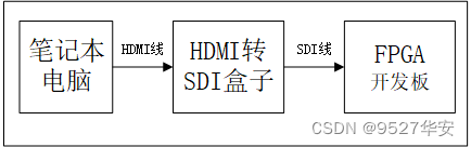
There are two SDI input devices, which are connected to the 2-way SDI video input interface of the FPGA development board; one is a 3G-SDI camera with a resolution of 1920x1080@60Hz, and HD-SDI or SD-SDI cameras can also be used, because this design is adaptive to three types of SDI videos; the other is an HDMI to 3G-SDI box, which is connected to a laptop to simulate an SDI camera; SDI cameras are relatively expensive, and friends with limited budgets can consider using an HDMI to SDI box to simulate an SDI camera, which costs about 100 yuan on Taobao; when using an HDMI to SDI box, the input source can be a laptop, that is, use a laptop to connect to the HDMI input interface of the HDMI to SDI box via an HDMI cable, and then use an SDI cable to connect the SDI output interface of the HDMI to SDI box to the FPGA development board, as follows:
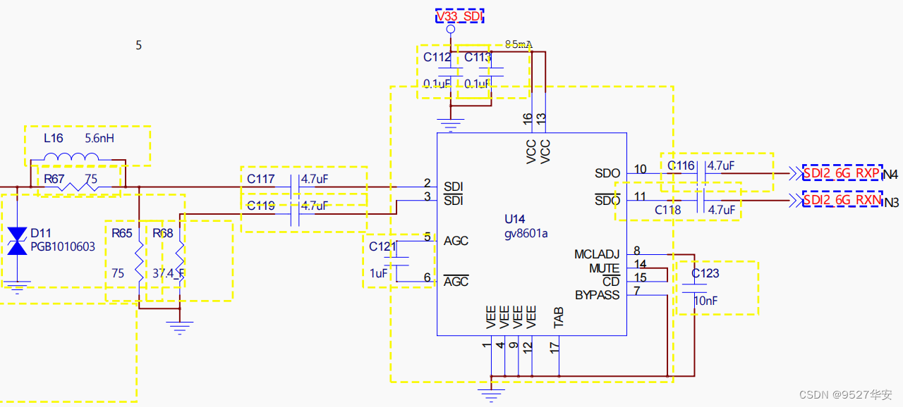
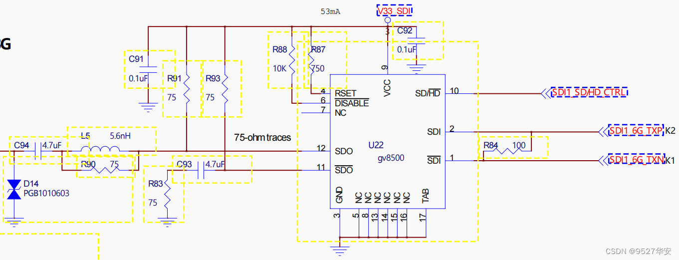
The Gv8601a chip realizes the functions of single-ended to differential and EQ. Gv8601a is selected here because it is based on the official solution of Xilinx. Of course, other models of devices can also be used. The schematic diagram of the Gv8601a equalizer is as follows:
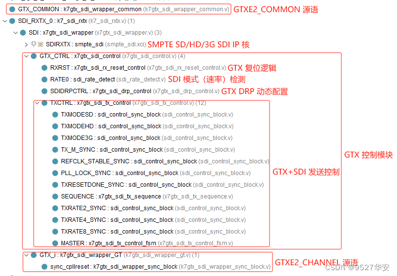
This design uses Xilinx's unique GTX high-speed signal processing resources to realize the deserialization and serialization of SDI differential video signals. For SDI video reception, GTX plays the role of deserialization, that is, deserializing the input high-speed serial differential signal into parallel digital signals; for SDI video transmission, GTX plays the role of serialization, that is, serializing the input parallel digital signal into a high-speed serial differential signal; the use of GTX generally requires instantiation of GTX The IP core is configured through the UI interface of vivado, but this design requires automatic identification and adaptive processing of SD-SDI, HD-SDI, and 3G-SDI videos, so GTX needs to have the function of dynamically changing the line rate. This function can be configured through the DRP interface or the rate interface of GTX. Therefore, it cannot be configured using the UI interface of vivado, but directly instantiates the GTXE2_CHANNEL and GTXE2_COMMON source language of GTX to directly use GTX resources; In addition, in order to dynamically configure the GTX line rate, a GTX control module is also required. This module refers to the official design of Xilinx and has functions such as dynamic monitoring of SDI mode and dynamic configuration of DRP; This solution refers to the official design of Xilinx; The code architecture of the GTX deserialization and serialization module is as follows:
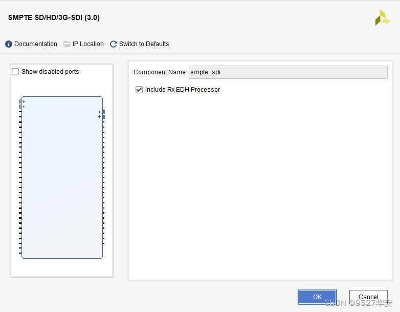
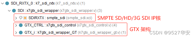
The SMPTE SD/HD/3G SDI IP core is a Xilinx series FPGA-specific IP for SDI video encoding and decoding. The IP configuration is very simple. The UI interface of vivado is as follows:
The SMPTE SD/HD/3G SDI IP core must be used in conjunction with GTX. For SDI video reception, the IP receives data from GTX and then decodes the SDI video into BT1120 video output. For SDI video transmission, the IP receives BT1120 video data from the user side and then encodes the BT1120 video into SDI video output. This solution refers to the official design of Xilinx. The SMPTE SD/HD/3G SDI IP core code architecture is as follows:
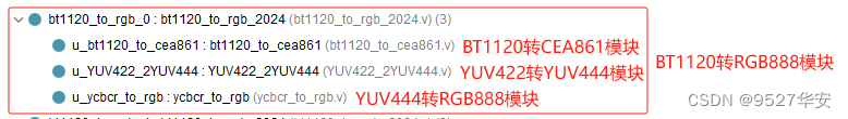
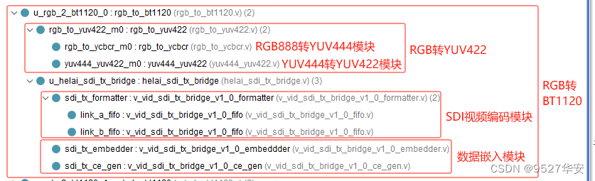
The function of the BT1120 to RGB module is to convert the BT1120 video decoded and output by the SMPTE SD/HD/3G SDI IP core into RGB888 video. It consists of three modules: BT1120 to CEA861 module, YUV422 to YUV444 module, and YUV444 to RGB888 module. This solution refers to the official design of Xilinx; the code architecture of the BT1120 to RGB module is as follows:
The video cache solution of this design adopts 2-way Xilinx official VDMA image cache architecture; the cache medium is PS end DDR3; the first channel SDI video is written to DDR through VDMA and then read out to the video fusion overlay module, and the second channel SDI video is not read out after being written to DDR through VDMA, but is read from DDR3 through the video fusion overlay module. Taking engineering source code 1 as an example, VDMA uses Xilinx vivado's Block Design design, as shown below:

To reduce latency, VDMA is set to cache 1 frame as follows:

The multi-channel video fusion overlay design block diagram is as follows:
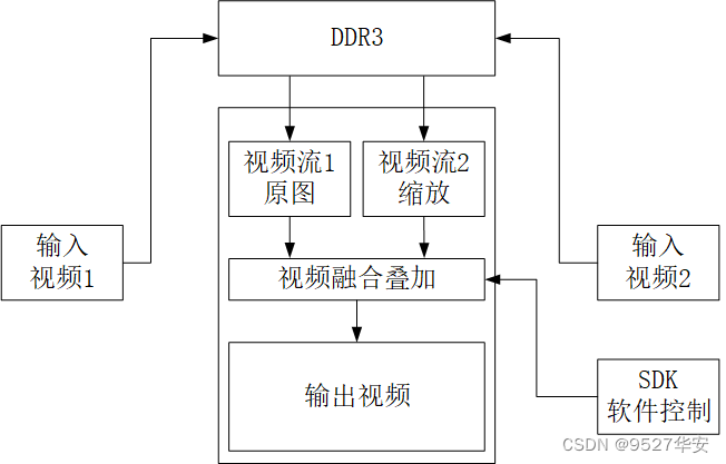
Multi-channel video fusion and overlay are formed by the fusion and overlay of the bottom video and the overlay video. The bottom video is the input video channel 1, and the overlay video is obtained after scaling the video channel 2. The two videos are fused together and output. The transparency of the fusion of the two videos, the scaling size of the overlay video, the display position of the overlay video and other information can be dynamically configured through the SDK software; the design is implemented in C++ code using the HLS solution, and is synthesized into RTL and encapsulated as IP, which can be called in vivado. For details of this solution, please refer to my previous blog, the blog link is as follows:
Click to go directly to
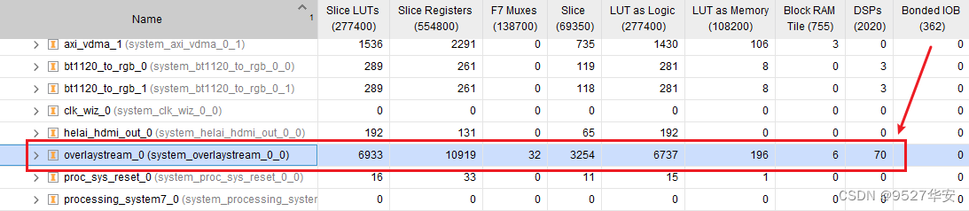
The comprehensive resource usage of this IP in vivado is as follows:
HLS multi-channel video fusion overlay requires running the driver and user program in the SDK to work properly. I have provided a C language program in the project. Please refer to the project source code for details. The screenshot of HLS multi-channel video fusion overlay call is as follows:

The HDMI video output architecture is as follows:

Referring to the official design of Xilinx, the VTC+AXI4-Stream To Video Out architecture is used to implement the conversion of the output video from AXI4-Stream to Native format; then the RGB888 to HDMI module implemented by pure Verilog code is used to implement the conversion from RGB888 to HDMI, and finally displayed on the monitor. The code architecture of the RGB888 to HDMI module is as follows:

For more information about the RGB888 to HDMI module, please refer to my previous blog:Click to go directly to
The SDI video output architecture must first implement the conversion of the AXI4-Stream read out by VDMA to the Native format, and then convert the RGB888 video to the BT1120 video through RGB to BT1120. The architecture is as follows:

In SDI output mode, the pixel clock of the VGA timing module is provided by the sending user clock of the SMPTE SD/HD/3G SDI IP core. The pixel clock is different in different SDI modes. For example, the pixel clock is 148.5M in 3G-SDI mode and 74.25M in HD-SDI 720P@60Hz mode.
In SDI output mode, an RGB to BT1120 module is required. The function of the RGB to BT1200 module is to convert the RGB video on the user side into BT1200 video and output it to the SMPTE SD/HD/3G SDI IP core. The RGB to BT1120 module consists of an RGB888 to YUV444 module, a YUV444 to YUV422 module, an SDI video encoding module, and a data embedding module. This solution refers to the official design of Xilinx. The code architecture of the BT1120 to RGB module is as follows:
These two parts share the corresponding modules with the receiving process, and are functionally the reverse process of the receiving process, so they will not be described in detail.
The Gv8500 chip realizes the functions of differential to single-ended conversion and enhanced drive. The Gv8500 is selected here because it draws on the official solution of Xilinx. Of course, other models of devices can also be used. The schematic diagram of the Gv8500 driver is as follows:
In SDI output mode, you need to use an SDI to HDMI box, because the monitor I have does not have an SDI interface, only an HDMI interface. In order to display SDI video, this is the only way. Of course, if your monitor has an SDI interface, you can directly connect the display. I bought my SDI to HDMI box on Taobao for less than 100 yuan.
This blog provides 2 sets of project source code. Taking project source code 1 as an example, the vivado Block Design is designed as follows. Other projects are similar. The Block Design is designed as part of the image cache architecture:

Taking project source code 1 as an example, the project source code structure is as follows. Other projects are similar:

The PL clock of the project source code is provided by the Zynq soft core, so you need to run the SDK to start Zynq. In addition, IP cores such as video fusion overlay and VDMA need to run software drivers to work properly. The SDK software code architecture is as follows:

The configuration in the SDK code is as follows, and users can modify it according to their needs;
The first video channel is the bottom layer video with a resolution of 1920x1080;
The second video is an overlay video with a resolution of 1920x1080. A 1000x800 area is taken from the overlay video coordinate (400,200) as the origin as the overlay fusion video.
Scale the 600x600 superimposed fusion video obtained in the previous step to 960x540;
Overlay the 960x540 superimposed fusion video in the previous step starting from the (0,0) coordinate of the underlying video, and set the transparency of the underlying and overlay layers to 80;
Development board FPGA model: Xilinx-Zynq7100–xc7z100ffg900-2;
Development environment: Vivado2019.1;
Input: 3G-SDI camera or HDMI to SDI box, resolution 1920x1080@60Hz;
Output: HDMI, resolution 1920x1080@60Hz;
Cache solution: Xilinx official VDMA solution;
Cache medium: PS side DDR3;
Video fusion and overlay solution: self-developed multi-channel video fusion and overlay based on HLS;
Project purpose: The purpose of this project is to enable readers to master the design capabilities of Zynq series FPGA to realize SDI to HDMI conversion, so as to be able to transplant and design their own projects;
For project block design and project code architecture, please refer to the "Project Source Code Architecture" section in Chapter 3;
The resource consumption and power consumption of the project are as follows:

Development board FPGA model: Xilinx-Zynq7100–xc7z100ffg900-2;
Development environment: Vivado2019.1;
Input: 3G-SDI camera or HDMI to SDI box, resolution 1920x1080@60Hz;
Output: 3G-SDI, resolution 1920x1080@60Hz;
Cache solution: Xilinx official VDMA solution;
Cache medium: PS side DDR3;
Video fusion and overlay solution: self-developed multi-channel video fusion and overlay based on HLS;
Project purpose: The purpose of this project is to enable readers to master the design capabilities of Zynq series FPGA to realize SDI to HDMI conversion, so as to be able to transplant and design their own projects;
For project block design and project code architecture, please refer to the "Project Source Code Architecture" section in Chapter 3;
The resource consumption and power consumption of the project are as follows:

1: If your vivado version is the same as the vivado version of this project, open the project directly;
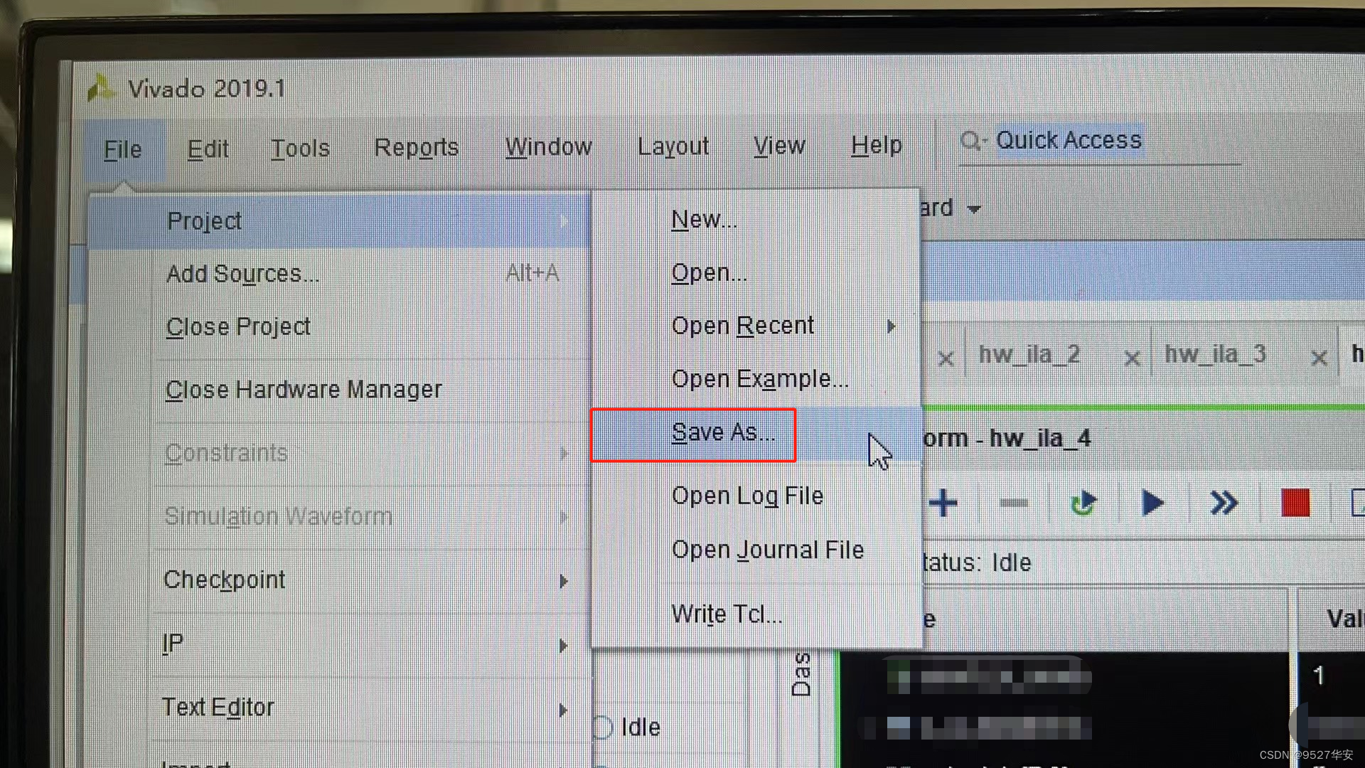
2: If your Vivado version is lower than the Vivado version of this project, you need to open the project and click File -> Save As. However, this method is not safe. The safest way is to upgrade your Vivado version to the Vivado version of this project or a higher version.
3: If your vivado version is higher than the vivado version of this project, the solution is as follows:
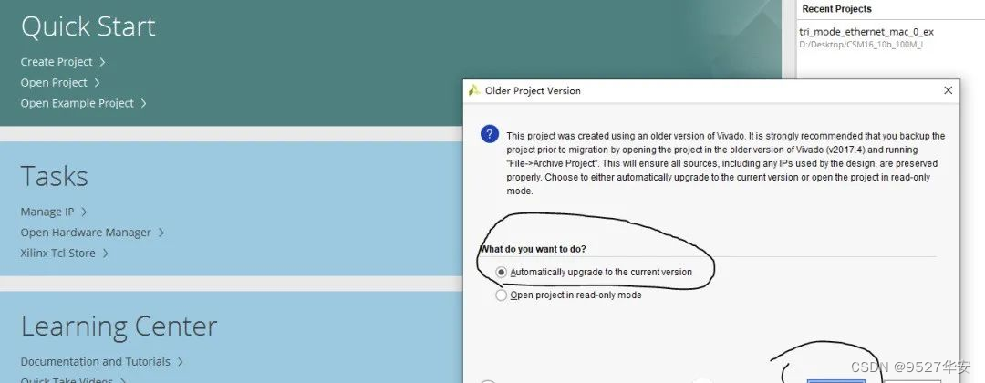
After opening the project, you will find that the IPs are locked, as follows:
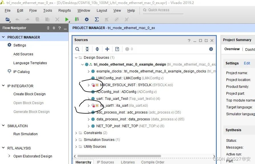
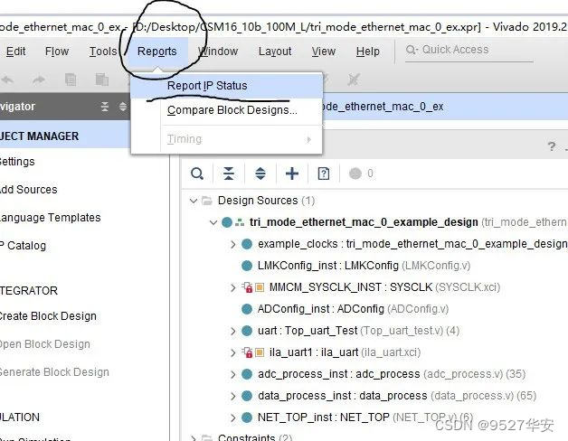
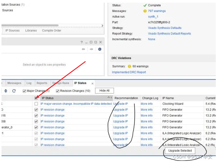
At this time, you need to upgrade the IP, the operation is as follows:
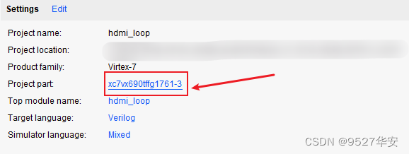
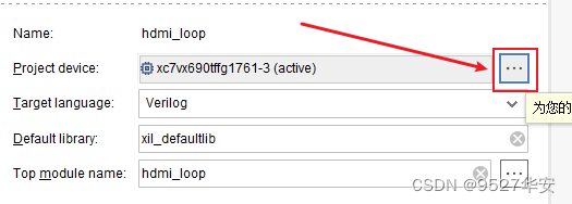
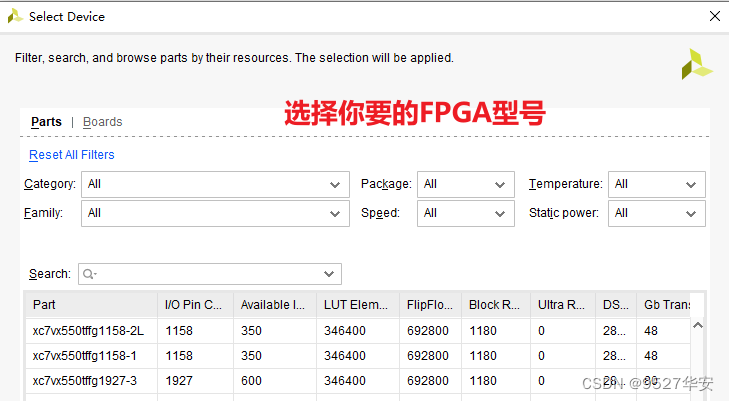
If your FPGA model is different from mine, you need to change the FPGA model as follows:
After changing the FPGA model, you also need to upgrade the IP. The method of upgrading the IP has been described above;
1: Since the DDR of each board may not be exactly the same, the MIG IP needs to be configured according to your own schematic diagram. You can even directly delete the MIG of my original project and re-add the IP and reconfigure it;
2: Modify the pin constraints according to your own schematic and modify them in the xdc file;
3: Pure FPGA migration to Zynq requires adding the zynq soft core to the project;
The equipment you need to prepare is as follows:
FPGA development board;
SDI camera or HDMI to SDI box;
SDI to HDMI box;
HDMI display;
My development board is connected as follows:

Taking project source code 1 as an example, the output is as follows:
Zynq-SDI-Video Fusion Overlay
Benefit: Access to engineering code
The code is too large to be sent via email, so I will send it via a network disk link.
How to obtain information: privately, or through the V business card at the end of the article.
The network disk information is as follows:

In addition, many friends have given this blogger a lot of comments and suggestions, hoping to enrich the service content and options. Because different friends have different needs, this blogger also provides the following services:


I have devoted myself to the research of technology for more than 30 years. I am proficient in various languages such as Java, Linux, JavaScript, PHP, CSS, etc. I have made many contributions in the field of open source. I have established a developer documentation site to share some problems in technology development for everyone to read.